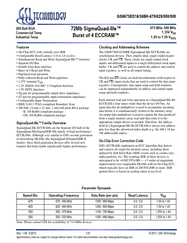
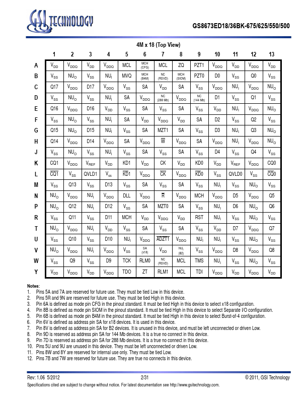
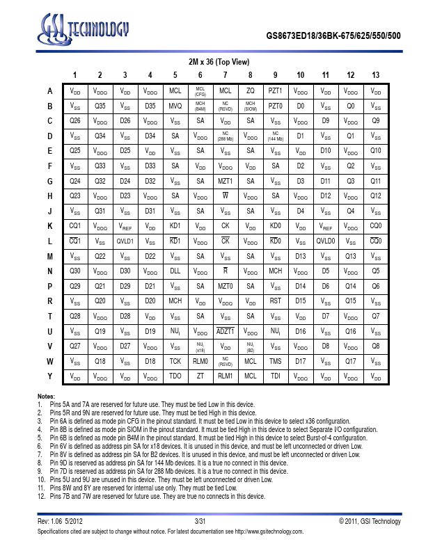
Description
Symbol
Description
SA
D[35:0]
Q[35:0]
QVLD[1:0] CK, CK
KD[1:0], KD[1:0] CQ[1:0], CQ[1:0]
Address
Read or Write Address is registered on ↑CK.
Registered on ↑KD and ↑KD during Write operations.
x18 and x36.
x36 only.
Driven by ↑CK and ↑CK, and synchronized with ↑CQ and ↑CQ during Read operations.
x18 and x36.
x36 only.
Driven high one half cycle before valid Re
Features
- On-Chip ECC with virtually zero SER.
- Configurable Read Latency (3.0 or 2.0 cycles).
- Simultaneous Read and Write SigmaQuad-IIIe™ Interface.
- Separate I/O Bus.
- Double Data Rate interface.
- Burst of 4 Read and Write.
- Pipelined read operation.
- Fully coherent Read and Write pipelines.
- 1.35V nominal VDD.
- 1.2V JESD8-16A BIC-3 Compliant Interface.
- 1.5V HSTL Interface.
- ZQ pin for programmable output.


