GSM6601 Overview
Key Features
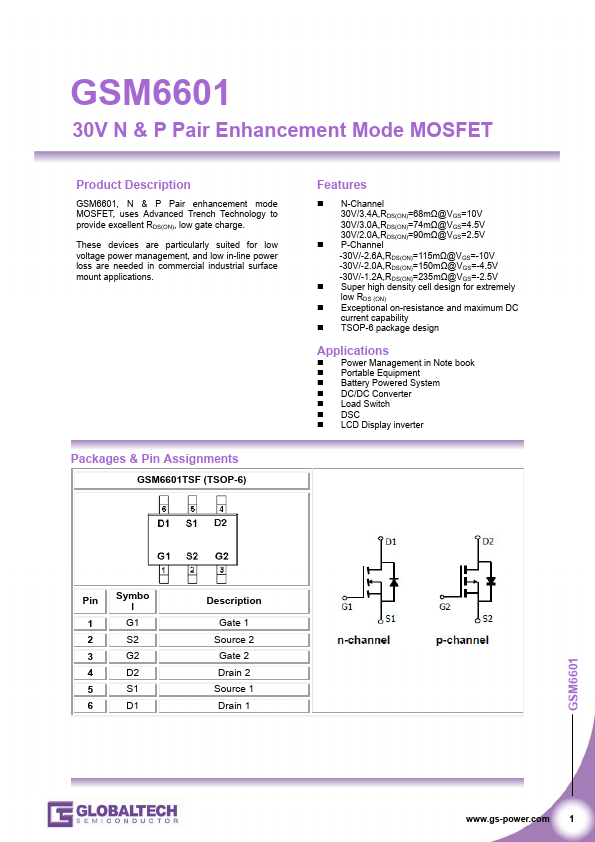
- N-Channel 30V/3.4A,RDS(ON)=68mΩ@VGS=10V 30V/3.0A,RDS(ON)=74mΩ@VGS=4.5V 30V/2.0A,RDS(ON)=90mΩ@VGS=2.5V
- P-Channel -30V/-2.6A,RDS(ON)=115mΩ@VGS=-10V -30V/-2.0A,RDS(ON)=150mΩ@VGS=-4.5V -30V/-1.2A,RDS(ON)=235mΩ@VGS=-2.5V
- Super high density cell design for extremely low RDS (ON)
- Exceptional on-resistance and maximum DC current capability
- TSOP-6 package design