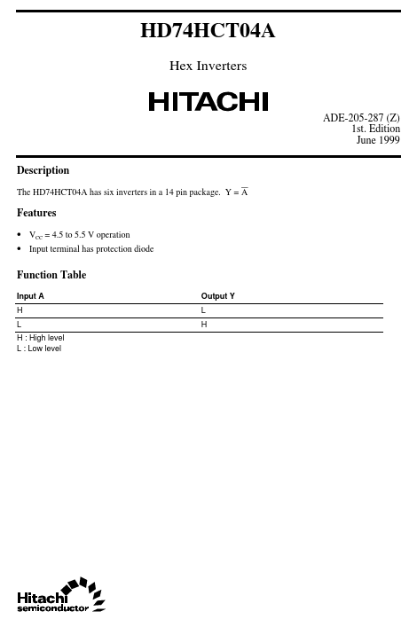
The HD74HCT04A has six inverters in a 14 pin package.
Features
VCC = 4.5 to 5.5 V operation.
Input terminal has protection diode
Function Table
Input A H L H : High level L : Low level Output Y L H
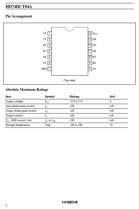
HD74HCT04A
Pin Arrangement
1A 1 1Y 2A 2 3
14 VCC 13 6A 12 6Y 11 5A 10 5Y 9 4A 8 4Y
2Y 4 3A 3Y 5 6
GND 7
(Top view)
Absolute Maximum Ratings
Item Supply voltage Input diode peak current Output diode peak current Output current VCC, GND current / pin Storage temperature Symbol VCC I IK I OK IO I CC or IGND Tstg Ratings.
HD74HCT1G04- High speed CMOS inverter using silicon gate CMOS process
HD74HCT237- 3-to-8-line Decoder/Demultiplexer with Address Latch
Full PDF Text Transcription
Click to expand full text
HD74HCT04A
Hex Inverters
ADE-205-287 (Z) 1st. Edition June 1999 Description
The HD74HCT04A has six inverters in a 14 pin package. Y = A
Features
• VCC = 4.5 to 5.5 V operation • Input terminal has protection diode
Function Table
Input A H L H : High level L : Low level Output Y L H
HD74HCT04A
Pin Arrangement
1A 1 1Y 2A 2 3
14 VCC 13 6A 12 6Y 11 5A 10 5Y 9 4A 8 4Y
2Y 4 3A 3Y 5 6
GND 7
(Top view)
Absolute Maximum Ratings
Item Supply voltage Input diode peak current Output diode peak current Output current VCC, GND current / pin Storage temperature Symbol VCC I IK I OK IO I CC or IGND Tstg Ratings –0.5 to 7.
 HD74HCT04A Datasheet