IW4019B
TECHNICAL DATA
Quad AND/OR Select Gate
High-Voltage Silicon-Gate CMOS
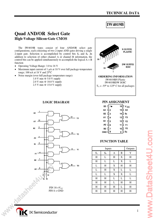
The IW4019B types consist of four AND/OR select gate configurations, each consisting of two 2-input AND gates driving a single 2-input gate. Selection is acplished by control bits Sa and Sb .In addition to selection of either channel A or channel B information, the control bits can be applied simultaneously to acplish the logical A + B function
- Operating Voltage Range: 3.0 to 18 V
- Maximum input current of 1 µA at 18 V over full package-temperature range; 100 n A at 18 V and 25°C
- Noise margin (over full package temperature range): 1.0 V min @ 5.0 V supply 2.0 V min @ 10.0 V supply 2.5 V min @ 15.0 V supply
ORDERING INFORMATION IW4019BN Plastic IW4019BDW SOIC TA = -55° to 125° C for all packages
LOGIC DIAGRAM
PIN ASSIGNMENT
FUNCTION TABLE
Inputs Sa H H L L L H H PIN 16 =VCC PIN 8 = GND H H Sb L L H H L H H H H A H L X X X L L H H B X X H L X L H L H Outputs Y H L H L L L H H H w w w
.d h s a t...