Description
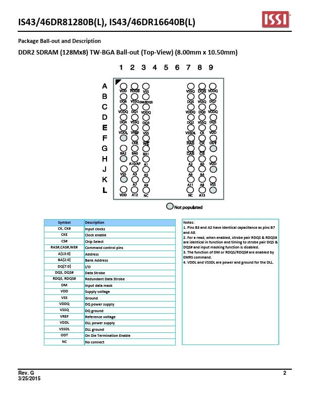
DDR2 SDRAM (128Mx8) TW-BGA Ball-out (Top-View) (8.00mm x 10.50mm)
Symbol CK, CK#
CKE CS# RAS#,CAS#,WE# A[13:0] BA[2:0] DQ[7:0] DQS, DQS# RDQS, RDQS# DM VDD VSS VDDQ VSSQ VREF VDDL VSSDL ODT NC
Description Input clocks Clock enable Chip Select Command control pins Address Bank Address I/O Data Strobe Redundant Data Strobe Input data mask Supply voltage Ground DQ power supply DQ ground Reference voltage DLL power supply DLL ground On Die Termination Enable No connect
Rev.G 3/25/2015
Notes: 1.
Features
- Clock frequency up to 400MHz.
- 8 internal banks for concurrent operation.
- 4-bit prefetch architecture.
- Programmable CAS Latency: 3, 4, 5, 6 and 7.
- Programmable Additive Latency: 0, 1, 2, 3, 4, 5
and 6.
- Write Latency = Read Latency-1.
- Programmable Burst Sequence: Sequential or
Interleave.
- Programmable Burst Length: 4 and 8.
- Automatic and Controlled Precharge Command.
- Power Down Mode.
- Auto Refresh and Self Refresh.
- Refresh Interval: 7.8 .
 IS46DR81280B-ISSI.pdf