Click to expand full text
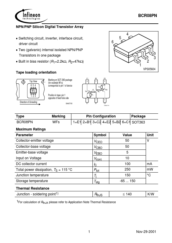
BCR08PN
NPN/PNP Silicon Digital Transistor Array
4
� Switching circuit, inverter, interface circuit,
5 6
driver circuit
� Two (galvanic) internal isolated NPN/PNP
Transistors in one package
� Built in bias resistor (R1=2.2k�, R2=47k�)
2 1
3
VPS05604
Tape loading orientation
Top View 654 W1s 123 Direction of Unreeling Position in tape: pin 1 opposite of feed hole side
EHA07193
Marking on SOT-363 package (for example W1s) corresponds to pin 1 of device
C1 6
B2 5
E2 4
R2 R1 TR1 R2 1 E1 2 B1 3 C2
EHA07176
TR2 R1
Type BCR08PN
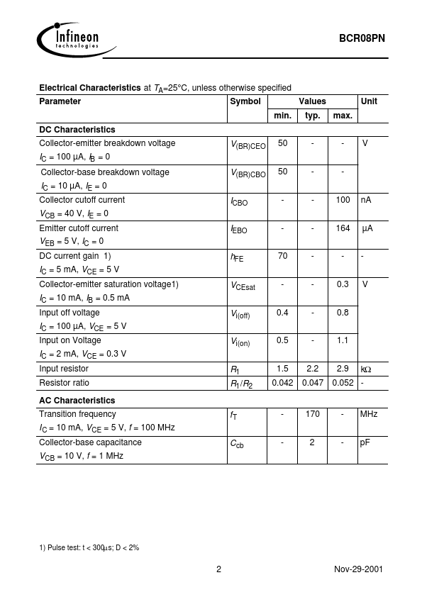
Maximum Ratings Parameter
Marking WFs
Pin Configuration
Package
1=E1 2=B1 3=C2 4=E2 5=B2 6=C1 SOT363
Symbol VCEO VCBO VEBO Vi(on) IC Ptot Tj Tstg
Value 50 50 5 10 100 250 150 -65 ...
 BCR08PN Datasheet