Datasheet4U Logo Datasheet4U.com

IDT5V2528 Datasheet - Integrated Device

2.5V / 3.3V PHASE-LOCK LOOP CLOCK DRIVER ZERO DELAY BUFFER

IDT5V2528 Features

* Operates at 3.3V VDD/AVDD and 2.5V/3.3V VDDQ

* 1:10 fanout

* 3-level inputs for output control

* External feedback (FBIN) pin is used to synchronize the outputs to the clock input signal

* No external RC network required for PLL loop stability

* Con

IDT5V2528 General Description

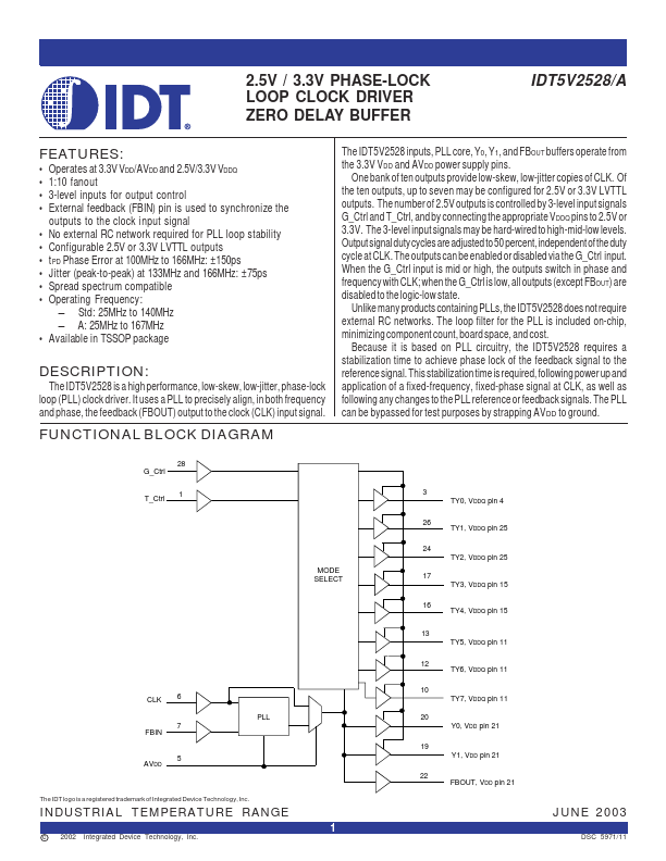
The IDT5V2528 is a high performance, low-skew, low-jitter, phase-lock loop (PLL) clock driver. It uses a PLL to precisely align, in both frequency and phase, the feedback (FBOUT) output to the clock (CLK) input signal. FUNCTIONAL BLOCK DIAGRAM The IDT5V2528 inputs, PLL core, Y0, Y1, and FBOUT buff.

IDT5V2528 Datasheet (58.65 KB)

Preview of IDT5V2528 PDF

Datasheet Details

Part number:

IDT5V2528

Manufacturer:

Integrated Device

File Size:

58.65 KB

Description:

2.5v / 3.3v phase-lock loop clock driver zero delay buffer.
IDT5V2528/A 2.5 / 3.3V PHASE-LOCK LOOP CLOCK DRIVER 2.5V / 3.3V PHASE-LOCK LOOP CLOCK DRIVER ZERO DELAY BUFFER INDUSTRIALTEMPERATURERANGE IDT5V2528/A.

📁 Related Datasheet

IDT5V2528A 2.5V / 3.3V PHASE-LOCK LOOP CLOCK DRIVER ZERO DELAY BUFFER (Integrated Device)

IDT5V2305 2.5V TO 3.3V HIGH PERFORMANCE CLOCK BUFFER (Integrated Device)

IDT5V2305 HIGH PERFORMANCE CLOCK BUFFER (Renesas)

IDT5V2310 2.5V TO 3.3V HIGH PERFORMANCE CLOCK BUFFER (Integrated Device Technology)

IDT5V2310 HIGH PERFORMANCE CLOCK BUFFER (Renesas)

IDT5V19EE604 EEPROM PROGRAMMABLE VCXO CLOCK GENERATOR (Renesas)

IDT5V40501 PLL CLOCK MULTIPLIER (IDT)

IDT5V40501 PLL CLOCK MULTIPLIER (Renesas)

IDT5V41065 2 OUTPUT PCIE GEN1/2 SYNTHESIZER (IDT)

IDT5V41066 4 OUTPUT PCIE GEN1/2 SYNTHESIZER (IDT)

TAGS

IDT5V2528 2.5V 3.3V PHASE-LOCK LOOP CLOCK DRIVER ZERO DELAY BUFFER Integrated Device

Image Gallery

IDT5V2528 Datasheet Preview Page 2 IDT5V2528 Datasheet Preview Page 3

IDT5V2528 Distributor