Datasheet Details
| Part number | IDT5V41068A |
|---|---|
| Manufacturer | Renesas ↗ |
| File Size | 326.97 KB |
| Description | PCIE GEN1/2/3 CLOCK MULTIPLEXER |
| Datasheet |
 IDT5V41068A-Renesas.pdf IDT5V41068A-Renesas.pdf
|
| Part number | IDT5V41068A |
|---|---|
| Manufacturer | Renesas ↗ |
| File Size | 326.97 KB |
| Description | PCIE GEN1/2/3 CLOCK MULTIPLEXER |
| Datasheet |
IDT5V41068A-Renesas.pdf
|
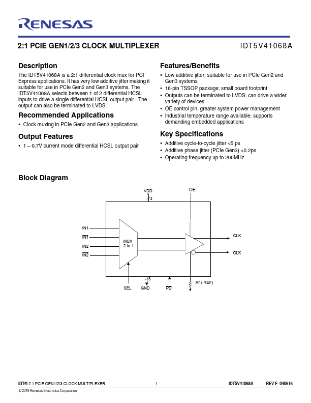
The IDT5V41068A is a 2:1 differential clock mux for PCI Express applications. Clock muxing in PCIe Gen2 and Gen3 applications Output
📁 IDT5V41068A Similar Datasheet