Datasheet Details
- Part number
- IDT72V255LA
- Manufacturer
- Integrated Device Tech
- File Size
- 196.61 KB
- Datasheet
- IDT72V255LA_IntegratedDeviceTechnology.pdf
- Description
- CMOS FIFO memories
IDT72V255LA Description
3.3 VOLT CMOS SuperSync FIFO™ 8,192 x 18 16,384 x 18 .IDT72V255LA Features
* IDT72V255LA IDT72V265LAIDT72V255LA Applications
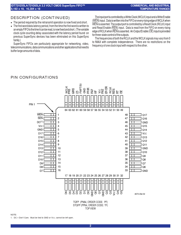
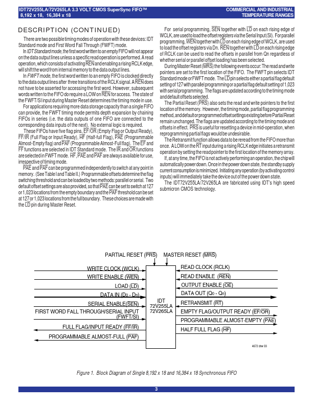
* that need to buffer large amounts of data. The input port is controlled by a Write Clock (WCLK) input and a Write Enable (WEN) input. Data is written into the FIFO on every rising edge of WCLK when WEN is asserted. The output port is controlled by a Read Clock (RCLK) input and Read Enable (REN) inp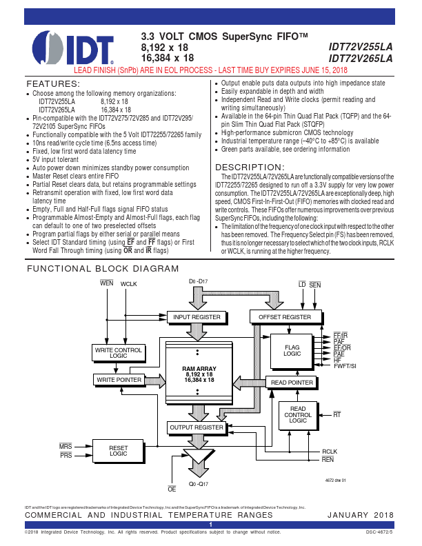
📁 Related Datasheet
📌 All Tags