Datasheet Details
| Part number | C5002 |
|---|---|
| Manufacturer | International |
| File Size | 127.01 KB |
| Description | Low Skew Muliple Frequency PCI Clock Generator with EMI Reducing SSCG |
| Datasheet |
 C5002 Datasheet C5002 Datasheet
|
|
|
| Part number | C5002 |
|---|---|
| Manufacturer | International |
| File Size | 127.01 KB |
| Description | Low Skew Muliple Frequency PCI Clock Generator with EMI Reducing SSCG |
| Datasheet |
C5002 Datasheet
|
|
|
|
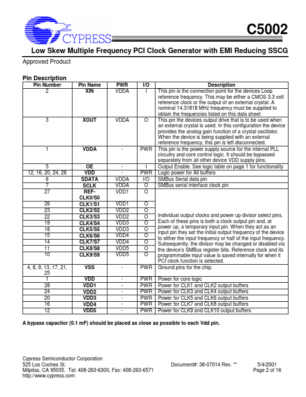
Pin Number 2 Pin Name XIN PWR VDDA I/O I Description This pin is the connection point for the devices Loop reference frequency.
📁 Similar Datasheet