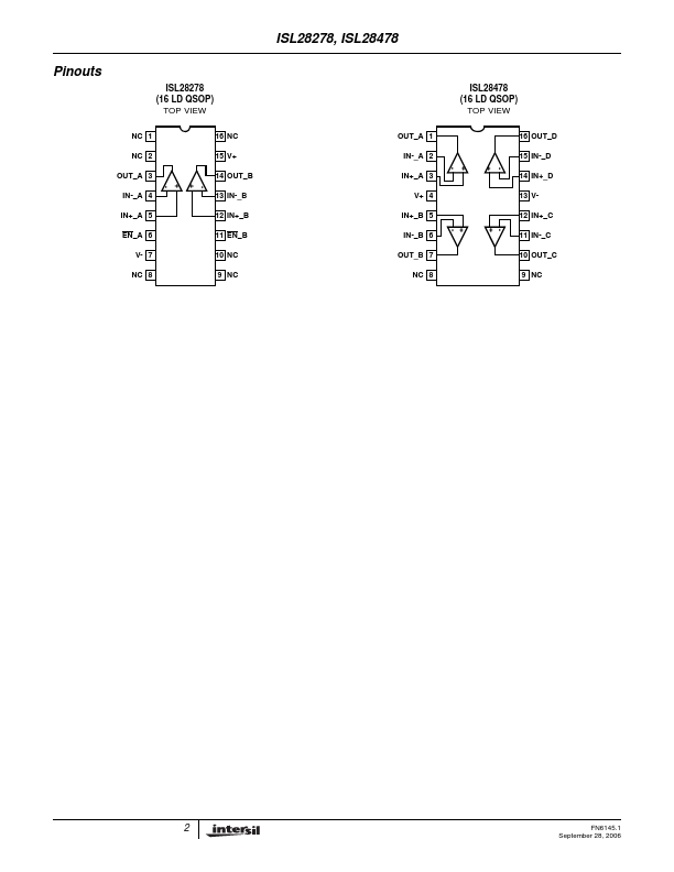
Description
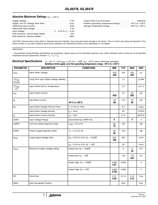
Input Offset Voltage Long Term Input Offset Voltage Stability Input Offset Drift vs Temperature Input Offset Current
MAX 225 450
UNIT µV µV/Mo µV/°C
1.2 2.2
±5
-600 Input Bias Current -40°C to +85°C Input Noise Voltage Peak-to-Peak Input Noise Voltage Density iN CMIR CMRR PSRR AVOL Input Noise Current Density Input Voltage Range Common-Mode Rejection Ratio Power Supply Rejection Ratio Large Signal Voltage Gain f = 0.1Hz to 10Hz fO = 1kHz fO = 1kHz Guaranteed by CMRR test VCM = 0V to 5V V+ =.
Features
- Low Power 120µA typ supply current for both channels.
- 225µV max offset voltage.
- 30pA typ input bias current.
- 300kHz gain-bandwidth product.
- 100dB typ PSRR and CMRR.
- Single supply operation down to 2.4V.
- Input is capable of swinging above V+ and below V(ground sensing).
- Rail-to-rail input and output (RRIO).
- Pb-free plus anneal available (RoHS compliant).