Datasheet4U Logo Datasheet4U.com

MT28C3212P2 - FLASH AND SRAM COMBO MEMORY

Datasheet Summary

Description

The MT28C3212P2FL and MT28C3212P2NFL combination Flash and SRAM memory devices provide a compact, low-power solution for systems where PCB real estate is at a premium.

Features

  • Flexible dual-bank architecture.
  • Support for true concurrent operations with no latency: Read bank b during program bank a and vice versa Read bank b during erase bank a and vice versa.
  • Organization: 2,048K x 16 (Flash) 128K x 16 (SRAM).
  • Basic configuration: Flash Bank a (4Mb Flash for data storage).
  • Eight 4K-word parameter blocks.
  • Seven 32K-word blocks Bank b (28Mb Flash for program storage).
  • Fifty-six 32K-word main blocks SRAM 2Mb.

📥 Download Datasheet

Datasheet preview – MT28C3212P2

Datasheet Details

Part number MT28C3212P2
Manufacturer MICRON
File Size 564.81 KB
Description FLASH AND SRAM COMBO MEMORY
Datasheet download datasheet MT28C3212P2 Datasheet
Additional preview pages of the MT28C3212P2 datasheet.
Other Datasheets by MICRON

Full PDF Text Transcription

Click to expand full text
2 MEG x 16 PAGE FLASH 128K x 16 SRAM COMBO MEMORY FLASH AND SRAM COMBO MEMORY FEATURES 
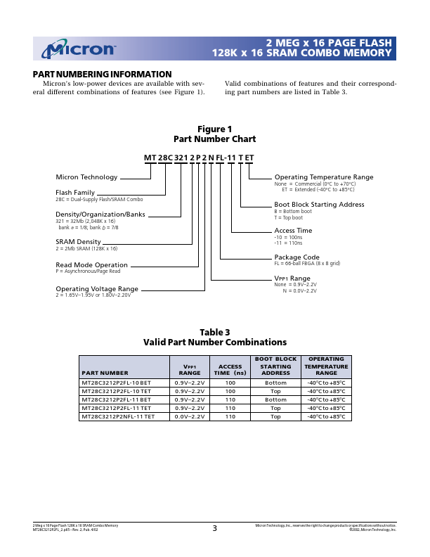
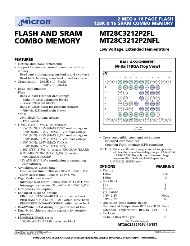
• Flexible dual-bank architecture • Support for true concurrent operations with no latency: Read bank b during program bank a and vice versa Read bank b during erase bank a and vice versa • Organization: 2,048K x 16 (Flash) 128K x 16 (SRAM) • Basic configuration: Flash Bank a (4Mb Flash for data storage) – Eight 4K-word parameter blocks – Seven 32K-word blocks Bank b (28Mb Flash for program storage) – Fifty-six 32K-word main blocks SRAM 2Mb SRAM for data storage – 128K-words • F_VCC, VCCQ, F_VPP, S_VCC voltages1 1.65V (MIN)/1.95V (MAX) F_VCC read voltage or 1.80V (MIN)/2.20V (MAX) F_VCC read voltage 1.65V (MIN)/1.95V (MAX) S_VCC read voltage or 1.80V (MIN)/2.20V (MAX) S_VCC read voltage 1.65V (MIN)/1.
Published: |