Datasheet Details
| Part number | MC100LVEL39 |
|---|---|
| Manufacturer | Motorola |
| File Size | 127.05 KB |
| Description | 2/4 /4/6 Clock Generation Chip |
| Datasheet |
 MC100LVEL39_MotorolaInc.pdf MC100LVEL39_MotorolaInc.pdf
|
| Part number | MC100LVEL39 |
|---|---|
| Manufacturer | Motorola |
| File Size | 127.05 KB |
| Description | 2/4 /4/6 Clock Generation Chip |
| Datasheet |
MC100LVEL39_MotorolaInc.pdf
|
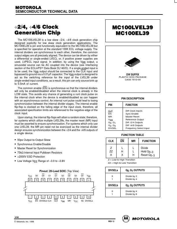
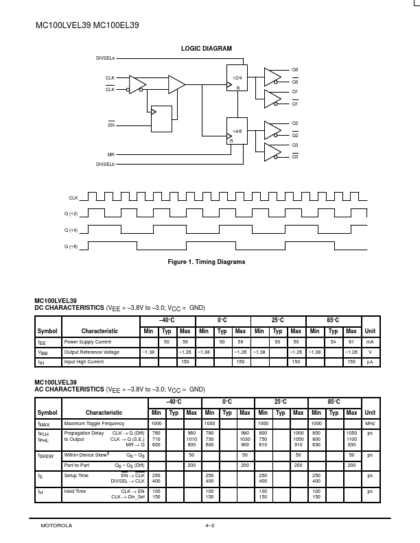
PIN CLK EN MR VBB Q0, Q1 Q2, Q3 DIVSEL FUNCTION Diff Clock Inputs Sync Enable Master Reset Reference Output Diff ÷2/4 Outputs Diff ÷4/6 Outputs Frequency Select Input FUNCTION TABLE CLK Z ZZ X EN L H X MR L L H FUNCTION Divide Hold Q0 3 Reset Q0 3 50ps Output-to-Output Skew Synchronous Enable/Disable Master Reset for Synchronization 75kΩ Internal Input Pulldown Resistors >2000V ESD Protection Low Voltage VEE Range of
📁 MC100LVEL39 Similar Datasheet