Description
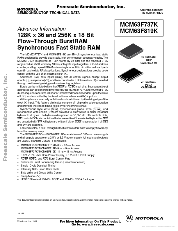
MOTOROLA Freescale Semiconductor, Inc.SEMICONDUCTOR TECHNICAL DATA Order this document by MCM63F737K/D Advance Information 128K x 36 and 256K x .
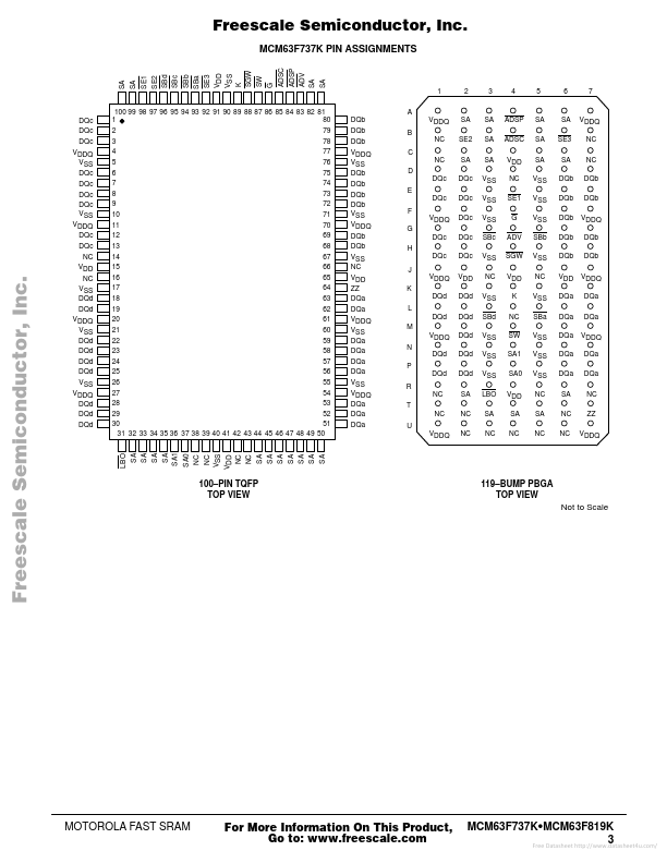
Pin Locations 85 Symbol ADSC Type Input Description Synchronous Address Status Controller: Active low, interrupts any ongoing burst and latches a new.
Features
* pt G, LBO, and ZZ. Linear Burst Order Input: This pin must remain in steady state (this signal not registered or latched). It must be tied high or low. Low
* linear burst counter. High
* interleaved burst counter. Synchronous Address Inputs: These inputs are reg
Applications
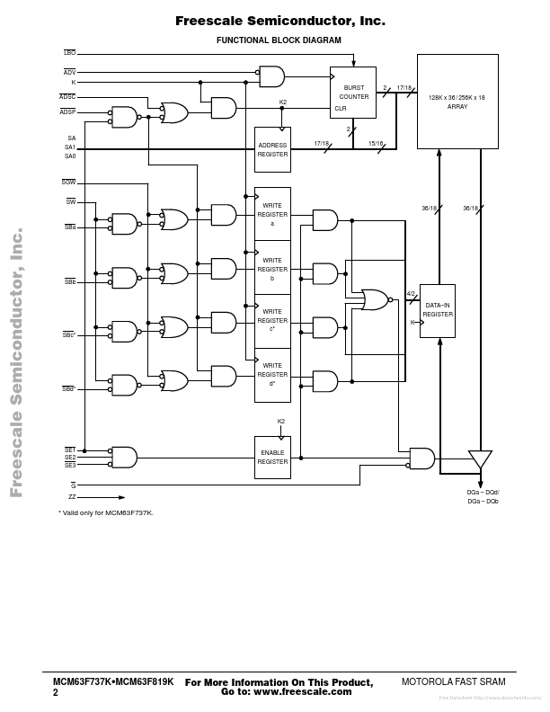
* Synchronous design allows precise cycle control with the use of an external clock (K). Addresses (SA), data inputs (DQx), and all control signals except output enable (G), sleep mode (ZZ), and linear burst order (LBO) are clock (K) controlled through positive
* edge
* triggered noninver