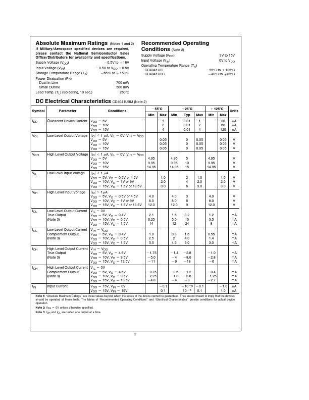
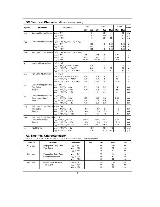
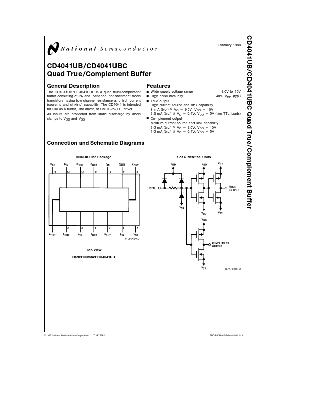
Datasheet4U Logo Datasheet4U.com

CD4041UB - Quad True/Complement Buffer

Datasheet Summary

Description

The CD4041UB CD4041UBC is a quad true complement buffer consisting of N- and P-channel enhancement mode transistors having low-channel resistance and high current (sourcing and sinking) capability The CD4041 is intended for use as a buffer line driver or CMOS-to-TTL driver All inputs are protected f

Features

  • Y Y Y Y Wide supply voltage range 3 0V to 15V High noise immunity 40% VDD (typ ) True output High current source and sink capability 8 mA (typ ) VO e 9 5V VDD e 10V 3 2 mA (typ ) VO e 0 4V VDD e 5V (two TTL loads) Complement output Medium current source and sink capability 3 6 mA (typ ) VO e 9 5V VDD e 10V 1 6 mA (typ ) VO e 0 4V VDD e 5V Connection and Schematic Diagrams Dual-In-Line Package 1 of 4 Identical Units TL F 5965.
  • 1 Top View Order Number CD4041UB TL F 5965.
  • 2.

📥 Download Datasheet

Datasheet preview – CD4041UB

Datasheet Details

Part number CD4041UB
Manufacturer National Semiconductor
File Size 118.74 KB
Description Quad True/Complement Buffer
Datasheet download datasheet CD4041UB Datasheet
Additional preview pages of the CD4041UB datasheet.
Other Datasheets by National Semiconductor

Full PDF Text Transcription

Click to expand full text
CD4041UB CD4041UBC Quad True Complement Buffer February 1988 CD4041UB CD4041UBC Quad True Complement Buffer General Description The CD4041UB CD4041UBC is a quad true complement buffer consisting of N- and P-channel enhancement mode transistors having low-channel resistance and high current (sourcing and sinking) capability The CD4041 is intended for use as a buffer line driver or CMOS-to-TTL driver All inputs are protected from static discharge by diode clamps to VDD and VSS Features Y Y Y Y Wide supply voltage range 3 0V to 15V High noise immunity 40% VDD (typ ) True output High current source and sink capability 8 mA (typ ) VO e 9 5V VDD e 10V 3 2 mA (typ ) VO e 0 4V VDD e 5V (two TTL loads) Complement output Medium current source and sink capability 3 6 mA (typ ) VO e 9 5V VDD e 10
Published: |