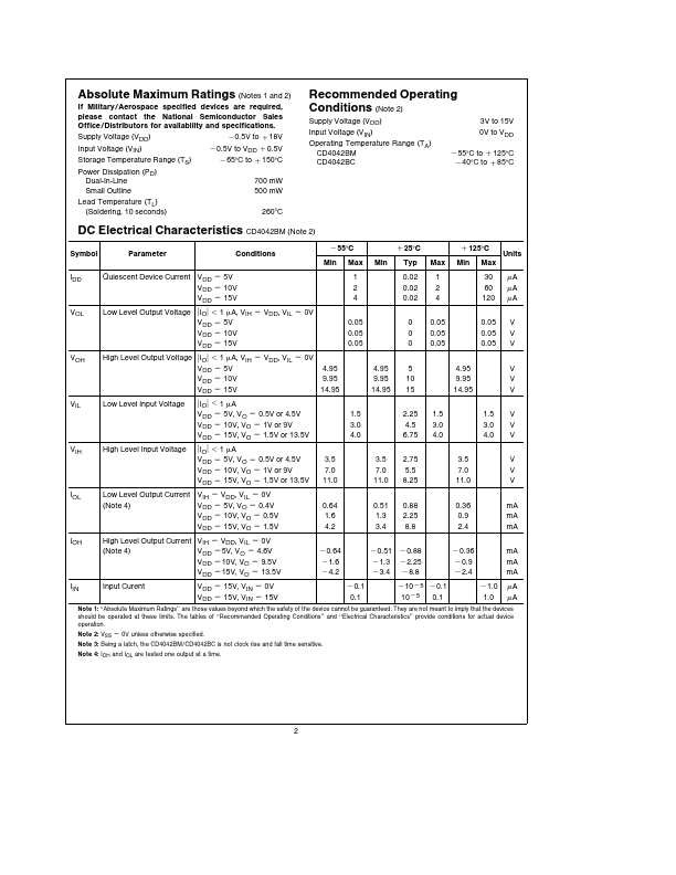
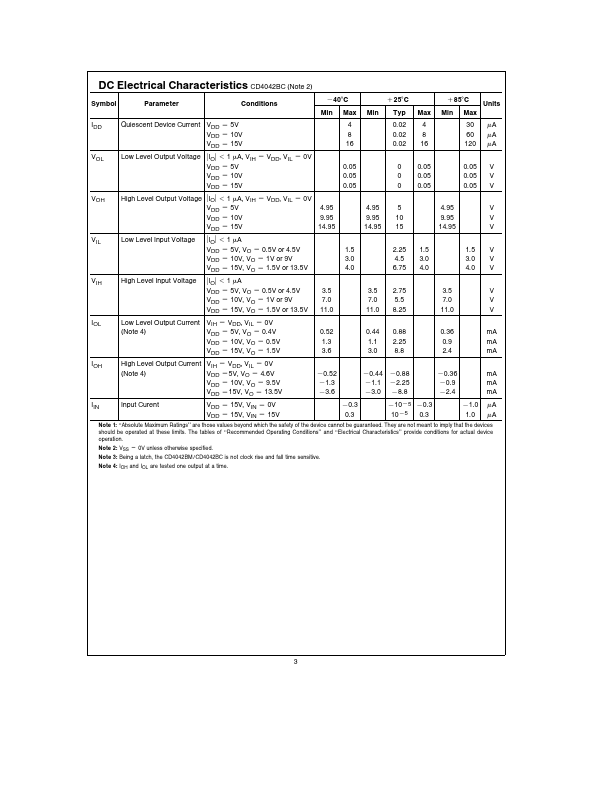
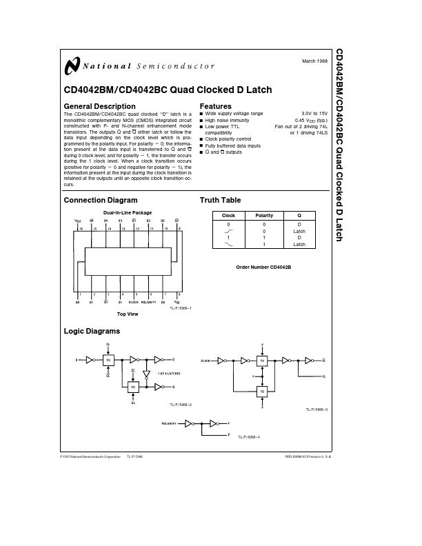
Datasheet4U Logo Datasheet4U.com

CD4042BC - Quad Clocked D-Latch

Datasheet Summary

Description

The CD4042BM CD4042BC quad clocked ‘‘D’’ latch is a monolithic complementary MOS (CMOS) integrated circuit constructed with P- and N-channel enhancement mode transistors The outputs Q and Q either latch or follow the data input depending on the clock level which is programmed by the polarity input F

Features

  • Y Y Y Y Y Y Wide supply voltage range High noise immunity Low power TTL compatibility Clock polarity control Fully buffered data inputs Q and Q outputs 3 0V to 15V 0 45 VDD (typ ) Fan out of 2 driving 74L or 1 driving 74LS Connection Diagram Dual-In-Line Package Truth Table Clock 0 L 1 K Polarity 0 0 1 1 Q D Latch D Latch Order Number CD4042B TL F 5966.
  • 1 Top View Logic Diagrams TL F 5966.
  • 2 TL F 5966.
  • 3 TL F 5966.
  • 4 C1995 National Semiconductor Co.

📥 Download Datasheet

Datasheet preview – CD4042BC
Other Datasheets by National Semiconductor

Full PDF Text Transcription

Click to expand full text
CD4042BM CD4042BC Quad Clocked D Latch March 1988 CD4042BM CD4042BC Quad Clocked D Latch General Description The CD4042BM CD4042BC quad clocked ‘‘D’’ latch is a monolithic complementary MOS (CMOS) integrated circuit constructed with P- and N-channel enhancement mode transistors The outputs Q and Q either latch or follow the data input depending on the clock level which is programmed by the polarity input For polarity e 0 the information present at the data input is transferred to Q and Q during 0 clock level and for polarity e 1 the transfer occurs during the 1 clock level When a clock transition occurs (positive for polarity e 0 and negative for polarity e 1) the information present at the input during the clock transition is retained at the outputs until an opposite clock transition oc
Published: |