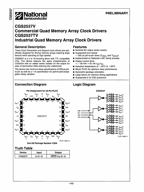
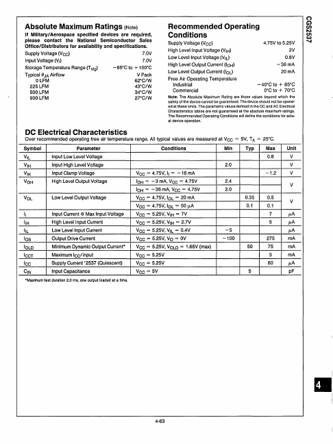
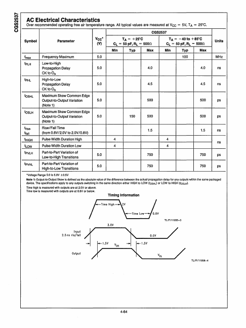
Datasheet Details
| Part number | CGS2537TV, CGS2537V |
|---|---|
| Manufacturer | National Semiconductor ↗ |
| File Size | 140.12 KB |
| Description | Industrial Quad Memory Array Clock Drivers |
| Datasheet |
 CGS2537V-NationalSemiconductor.pdf CGS2537V-NationalSemiconductor.pdf
|
| Note |
This datasheet PDF includes multiple part numbers: CGS2537TV, CGS2537V. Please refer to the document for exact specifications by model. |