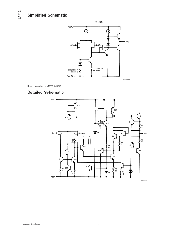
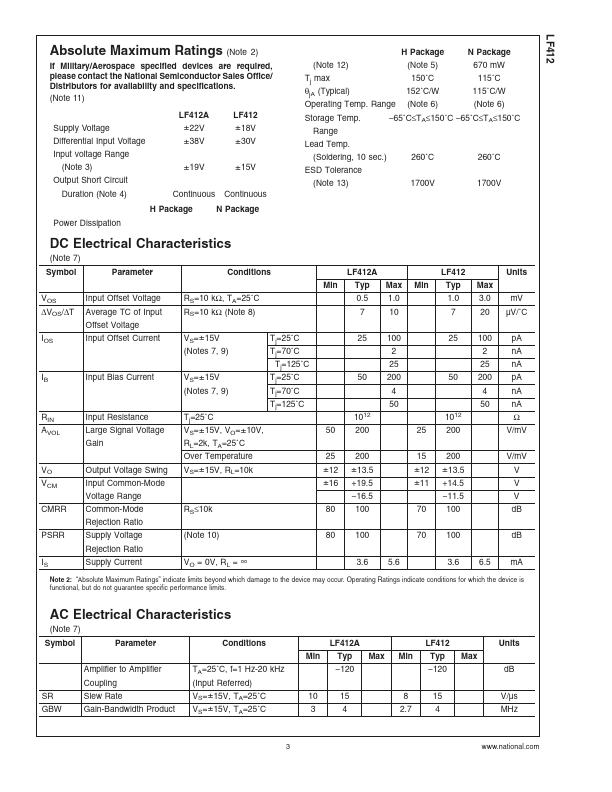
Datasheet Details
| Part number | LF412 |
|---|---|
| Manufacturer | National Semiconductor (now Texas Instruments) |
| File Size | 565.24 KB |
| Description | Low Offset/ Low Drift Dual JFET Input Operational Amplifier |
| Datasheet |
 LF412 Datasheet LF412 Datasheet
|
|
|
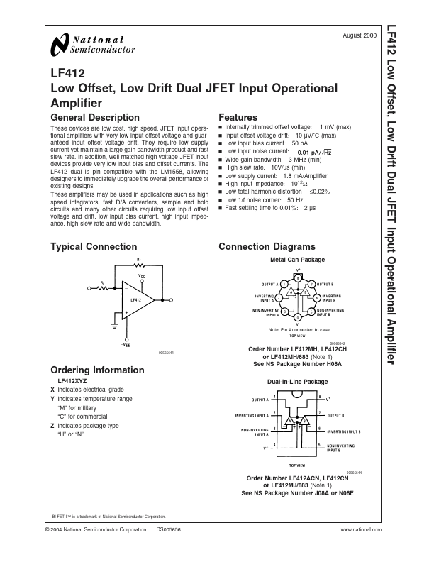
These devices are low cost, high speed, JFET input operational amplifiers with very low input offset voltage and guaranteed input offset voltage drift.
They require low supply current yet maintain a large gain bandwidth product and fast slew rate.
| Part number | LF412 |
|---|---|
| Manufacturer | National Semiconductor (now Texas Instruments) |
| File Size | 565.24 KB |
| Description | Low Offset/ Low Drift Dual JFET Input Operational Amplifier |
| Datasheet |
LF412 Datasheet
|
|
|
|