Datasheet Details
| Part number | MC100LVEL39 |
|---|---|
| Manufacturer | ON Semiconductor |
| File Size | 141.03 KB |
| Description | Clock Generation Chip |
| Datasheet |
 MC100LVEL39_ONSemiconductor.pdf MC100LVEL39_ONSemiconductor.pdf
|
|
|
The MC100LVEL39 by ON Semiconductor is a Clock Generation Chip. Below is the official datasheet preview.
| Part number | MC100LVEL39 |
|---|---|
| Manufacturer | ON Semiconductor |
| File Size | 141.03 KB |
| Description | Clock Generation Chip |
| Datasheet |
MC100LVEL39_ONSemiconductor.pdf
|
|
|
|
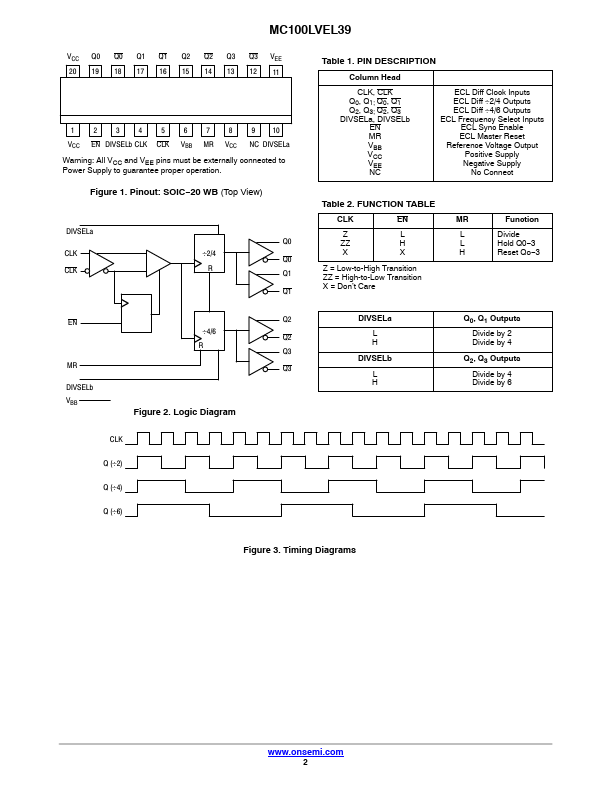
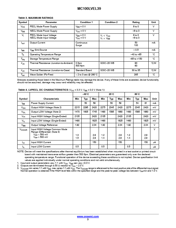
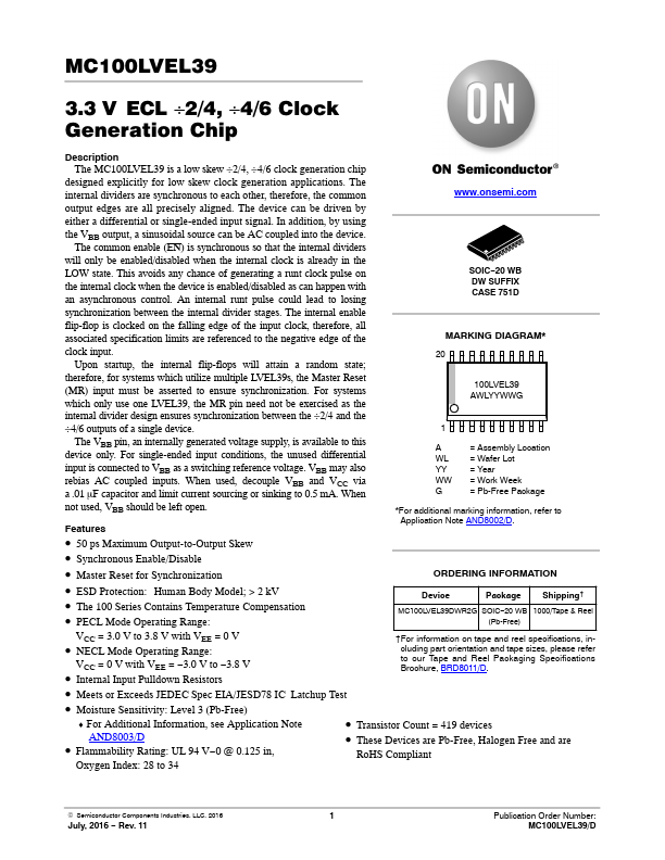
The MC100LVEL39 is a low skew ÷2/4, ÷4/6 clock generation chip designed explicitly for low skew clock generation applications.The internal dividers are synchronous to each other, therefore, the common output edges are all precisely aligned.The device can be driven by either a differential or single-ended input signal.In addition, by using the VBB output, a sinusoidal source can be AC coupled into the device.The common enable (EN) is synchronous so that the internal dividers will only be enab
📁 MC100LVEL39 Similar Datasheet