Datasheet Details
| Part number | NB3RL02 |
|---|---|
| Manufacturer | ON Semiconductor |
| File Size | 277.47 KB |
| Description | Low Phase-Noise Two-Channel Clock Fanout Buffer |
| Datasheet |
 NB3RL02_ONSemiconductor.pdf NB3RL02_ONSemiconductor.pdf
|
|
|
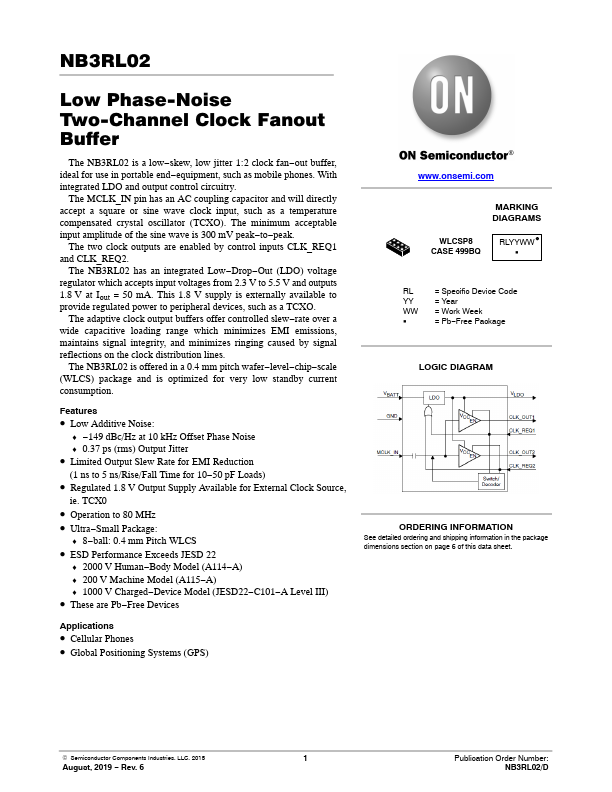
The NB3RL02 by ON Semiconductor is a Low Phase-Noise Two-Channel Clock Fanout Buffer. Below is the official datasheet preview.
| Part number | NB3RL02 |
|---|---|
| Manufacturer | ON Semiconductor |
| File Size | 277.47 KB |
| Description | Low Phase-Noise Two-Channel Clock Fanout Buffer |
| Datasheet |
NB3RL02_ONSemiconductor.pdf
|
|
|
|
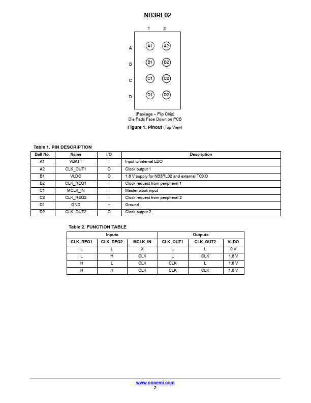
Ball No. Ground O Clock output 2 Table 2. FUNCTION TABLE Inputs CLK_REQ1 CLK_REQ2 L L L H H L H H MCLK_IN X CLK CLK CLK CLK_OUT1 L L CLK CLK Outputs CLK_OUT2 L C
📁 NB3RL02 Similar Datasheet