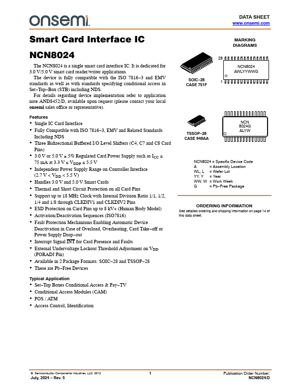
Description
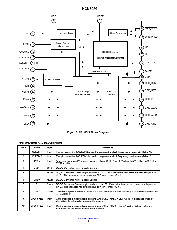
Pin #
Name
Type
Description
1
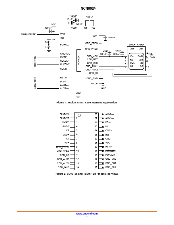
CLKDIV1 Input This pin coupled with CLKDIV2 is used to program the clock frequency division ratio (Table 1).2
CLKDIV2 Input This pin coupled with CLKDIV1 is used to program the clock frequency division ratio (Table 1).3
5V/3V
Input Allows selecting card VCC power supply voltage.CRD_VCC = 5 V when 5V/3V = HIGH or 3 V when
5V/3V = LOW
4
GNDP
GND DC/DC Converter Power Supply Ground
5
C2
Power DC/DC Converter Capacitor pin number 2
A 100 n
Features
- Single IC Card Interface.
- Fully Compatible with ISO 7816.
- 3, EMV and Related Standards
Including NDS.
- Three Bidirectional Buffered I/O Level Shifters (C4, C7 and C8 Card
Pins).
- 3.0 V or 5.0 V 5% Regulated Card Power Supply such as ICC
75 mA at 3.3 V VDDP 5.5 V.
- Independent Power Supply Range on Controller Interface
(2.7 V < VDD < 5.5 V).
- Handles 3.0 V and 5.0 V Smart Cards.
- Thermal and Short Circuit Protection on all Card Pins.
- Support up t.
 NCN8024_ONSemiconductor.pdf