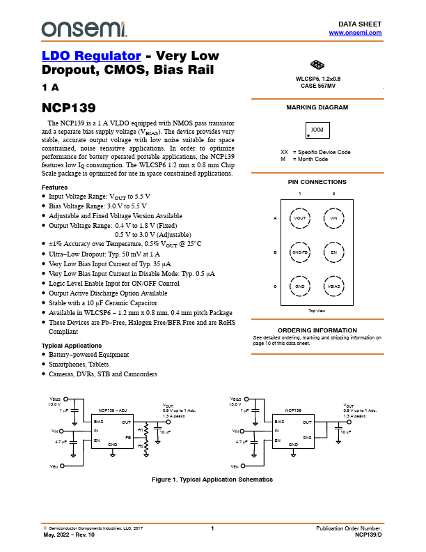
Datasheet Details
| Part number | NCP139 |
|---|---|
| Manufacturer | ON Semiconductor ↗ |
| File Size | 536.42 KB |
| Description | LDO Regulator |
| Datasheet |
 NCP139-ONSemiconductor.pdf NCP139-ONSemiconductor.pdf
|
| Part number | NCP139 |
|---|---|
| Manufacturer | ON Semiconductor ↗ |
| File Size | 536.42 KB |
| Description | LDO Regulator |
| Datasheet |
NCP139-ONSemiconductor.pdf
|
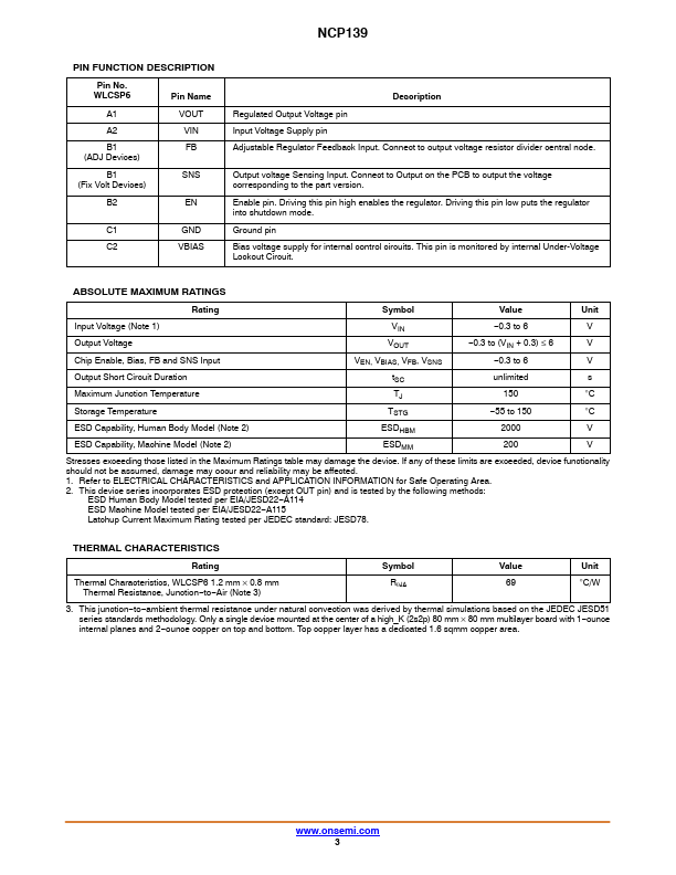
Pin No.
📁 NCP139 Similar Datasheet