Datasheet Details
| Part number | NCP398 |
|---|---|
| Manufacturer | ON Semiconductor ↗ |
| File Size | 680.71 KB |
| Description | USB Type-C VCONN Overvoltage Protection IC |
| Datasheet |
 NCP398-ONSemiconductor.pdf NCP398-ONSemiconductor.pdf
|
| Part number | NCP398 |
|---|---|
| Manufacturer | ON Semiconductor ↗ |
| File Size | 680.71 KB |
| Description | USB Type-C VCONN Overvoltage Protection IC |
| Datasheet |
NCP398-ONSemiconductor.pdf
|
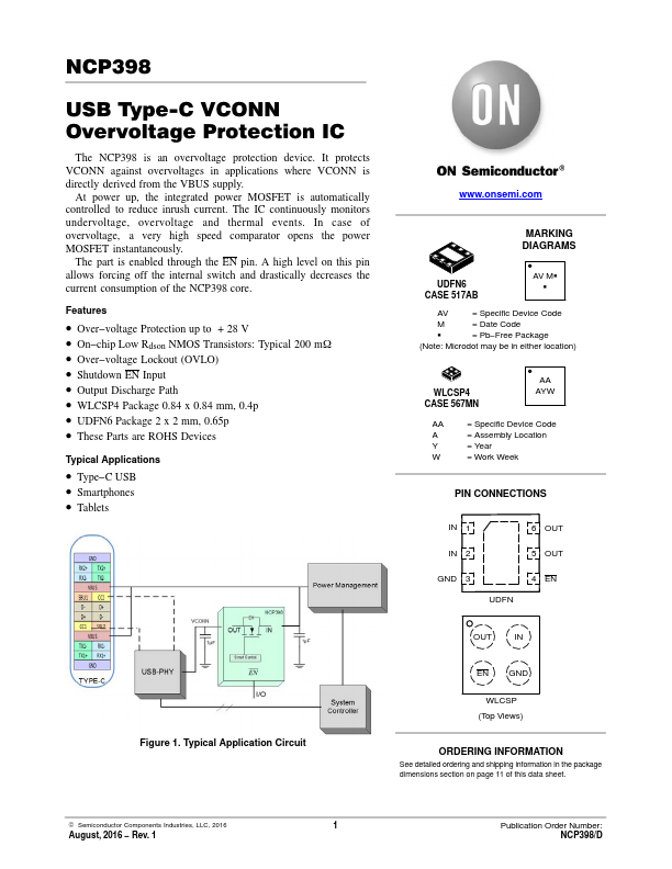
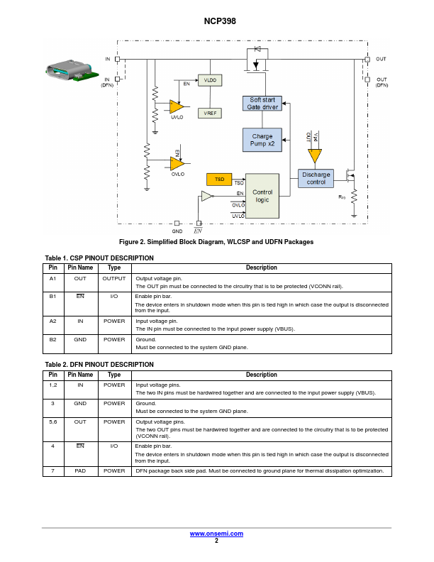
Pin Pin Name Type Description A1 OUT OUTPUT Output voltage pin.The OUT pin must be connected to the circuitry that is to be protected (VCONN rail).B1 EN I/O Enable pin bar.The device enters in shutdown mode when this pin is tied high in which case the output is disconnected from the input.A2 IN POWER Input voltage pin.The IN pin must be connected to the input power supply (VBUS).B2 GND POWER Ground.Must be connected to the system GND plane.Table 2. DFN PINOUT DESCRIP
📁 NCP398 Similar Datasheet