Datasheet Details
| Part number | NCV3020A |
|---|---|
| Manufacturer | ON Semiconductor ↗ |
| File Size | 773.03 KB |
| Description | Synchronous PWM Controller |
| Datasheet |
 NCV3020A-ONSemiconductor.pdf NCV3020A-ONSemiconductor.pdf
|
| Part number | NCV3020A |
|---|---|
| Manufacturer | ON Semiconductor ↗ |
| File Size | 773.03 KB |
| Description | Synchronous PWM Controller |
| Datasheet |
NCV3020A-ONSemiconductor.pdf
|
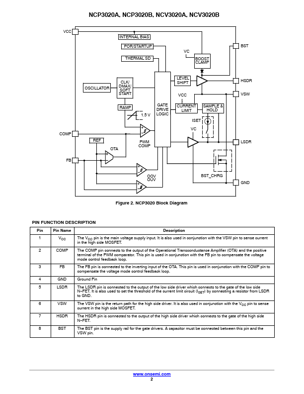
Pin Pin Name Description 1 VCC The VCC pin is the main voltage supply input.It is also used in conjunction with the VSW pin to sense current in the high side MOSFET.2 COMP The COMP pin connects to the output of the Operational Transconductance Amplifier (OTA) and the positive terminal of the PWM comparator.This pin is used in conjunction with the FB pin to compensate the voltage mode control feedback loop.3 FB The FB pin is connected to the inverting input of the OTA.This pin is used i
📁 NCV3020A Similar Datasheet