Datasheet4U Logo Datasheet4U.com

NCV51190 Datasheet - ON Semiconductor

NCV51190 1.5A DDR Memory Termination Regulator

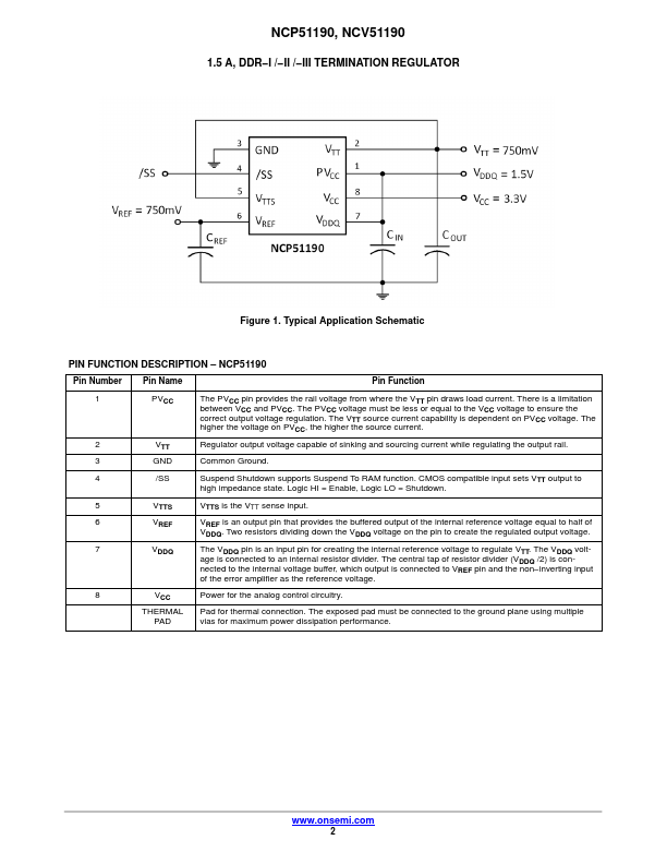
* NCP51190 Pin Number Pin Name Pin Function 1 PVCC The PVCC pin provides the rail voltage from where the VTT pin draws load current. There is a limitation between VCC and PVCC. The PVCC voltage must be less or equal to the VCC voltage to ensure the correct output voltage regulation. T.
NCP51190, NCV51190 1.5A DDR Memory Termination Regulator The NCP/NCV51190 is a simple, cost effective, high speed linear regulator designed to generate the VTT termination voltage rail for DDR I, DDR II and DDR III memory. The regulator is capable of actively sourcing or sinking up to ±1.5 A for DDR I, or up to ±0.5 A for DDR II / III while regulating the output voltage to within ±30 mV. The output termination voltage is tightly re.

NCV51190 Features

* include extremely low initial offset voltage, excellent load regulation, source/sink soft

* start and on

* chip thermal shut

* down protection. The NCP/NCV51190 features the power

* saving Suspend To Ram (STR) function which will tri

* state the regulator output and low

NCV51190 Datasheet (105.70 KB)

Preview of NCV51190 PDF
NCV51190 Datasheet Preview Page 2 NCV51190 Datasheet Preview Page 3

Datasheet Details

Part number:

NCV51190

Manufacturer:

ON Semiconductor ↗

File Size:

105.70 KB

Description:

1.5a ddr memory termination regulator.

📁 Related Datasheet

NCV51198 1.5A DDR Memory Termination Regulator (ON Semiconductor)

NCV51199 Termination Regulator (ON Semiconductor)

NCV511 Low-Dropout Voltage Regulator (ON Semiconductor)

NCV51152 Single Channel Gate Driver (ON Semiconductor)

NCV51153 4.5-A/9-A Isolated Single Channel Gate Driver (onsemi)

NCV5104 Half Bridge Driver (ON Semiconductor)

NCV5106A 600V Automotive High and Low Side Driver (ON Semiconductor)

NCV5106B 600V Automotive High and Low Side Driver (ON Semiconductor)

TAGS

NCV51190 1.5A DDR Memory Termination Regulator ON Semiconductor

NCV51190 Distributor