Datasheet Details
| Part number | NCV5707A |
|---|---|
| Manufacturer | ON Semiconductor ↗ |
| File Size | 435.91 KB |
| Description | High Current IGBT/MOSFET Gate Drivers |
| Datasheet |
 NCV5707A-ONSemiconductor.pdf NCV5707A-ONSemiconductor.pdf
|
| Part number | NCV5707A |
|---|---|
| Manufacturer | ON Semiconductor ↗ |
| File Size | 435.91 KB |
| Description | High Current IGBT/MOSFET Gate Drivers |
| Datasheet |
NCV5707A-ONSemiconductor.pdf
|
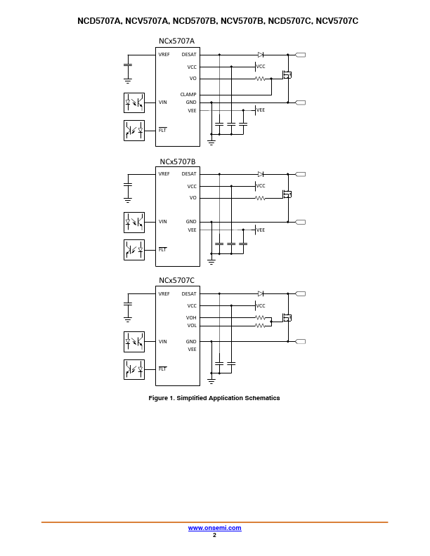
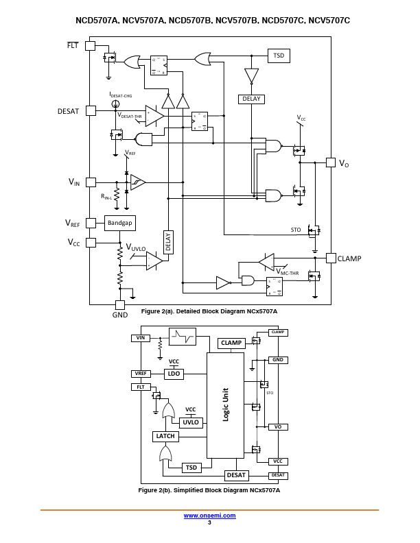
Pin Name No.I/O/x Description VIN 1 I Input signal to control the output.In applications which require galvanic isolation, VIN is generat- ed at the opto output, the pulse transformer secondary or the digital isolator output.VO (VOH/ VOL) signal is in phase with VIN.VIN is internally clamped to GND and has a pull down resistor of 1 MW to ensure that an output is low in the absence of an input signal.A minimum pulse width is required at VIN before VO (VOH/VOL) is
📁 NCV5707A Similar Datasheet