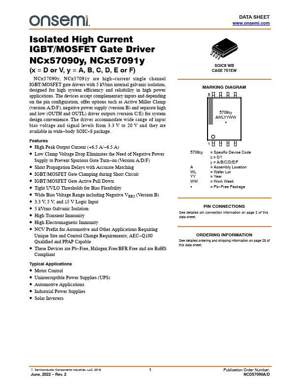
Description
Pin Name
No.I/O
Description
VDD1
1
Power Input side power supply.A good quality bypassing capacitor is required from this pin to GND1
and should be placed close to the pins for best results.The under voltage lockout (UVLO) circuit enables the device to operate at power on when
a typical supply voltage higher than VUVLO1
OUT
ON is present.
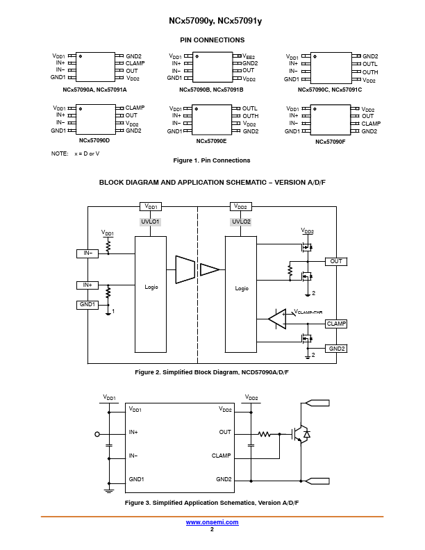
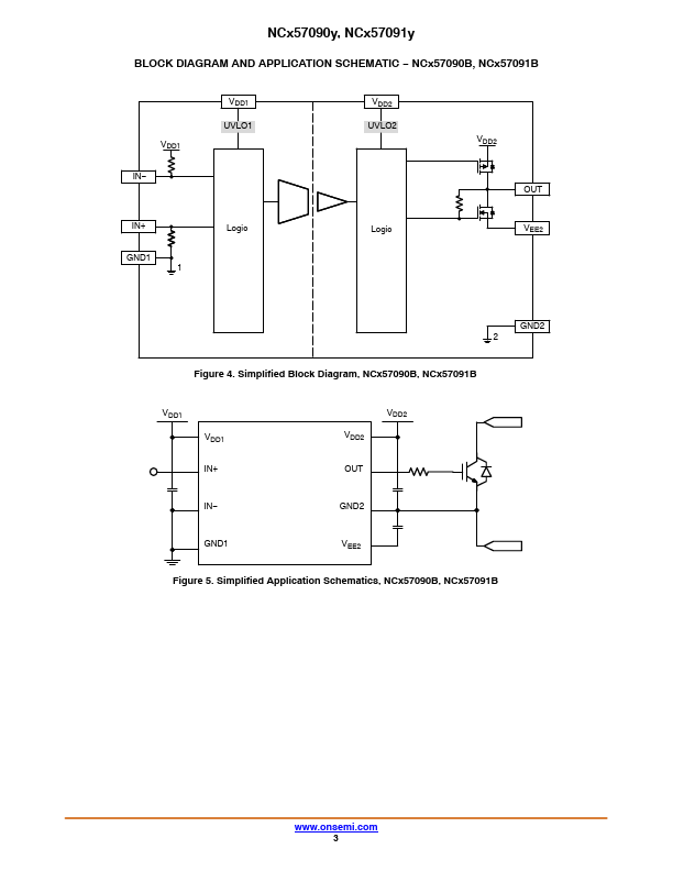
Features
- High Peak Output Current (+6.5 A/.
- 6.5 A).
- Low Clamp Voltage Drop Eliminates the Need of Negative Power
Supply to Prevent Spurious Gate Turn.
- on (Version A/D/F).
- Short Propagation Delays with Accurate Matching.
- IGBT/MOSFET Gate Clamping during Short Circuit.
- IGBT/MOSFET Gate Active Pull Down.
- Tight UVLO Thresholds for Bias Flexibility.
- Wide Bias Voltage Range including Negative VEE2 (Version B).
- 3.3 V, 5 V, an.
 NCV57090A-ONSemiconductor.pdf