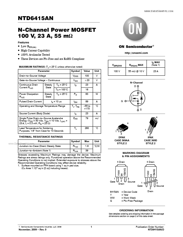
NTD6415AN
Features
- -
- -
Low RDS(on) High Current Capability 100% Avalanche Tested These Devices are Pb- Free and are Ro HS pliant
V(BR)DSS Value 100 $20 23 16 PD IDM TJ, Tstg IS EAS 83 89
- 55 to +175 23 79 W A °C G Unit V V A 100 V http://onsemi.
ID MAX (Note 1) 23 A
MAXIMUM RATINGS (TJ = 25°C unless otherwise noted)
Parameter Drain- to- Source Voltage Gate- to- Source Voltage
- Continuous Continuous Drain Current Rq JC Power Dissipation Rq JC Pulsed Drain Current Steady State Steady State TC = 25°C TC = 100°C TC = 25°C Symbol VDSS VGS ID
RDS(on) MAX 55 m W @ 10 V
N- Channel D tp = 10 ms
Operating and Storage Temperature Range Source Current (Body Diode) Single Pulse Drain- to- Source Avalanche Energy (VDD = 50 Vdc, VGS = 10 Vdc, IL(pk) = 23 A, L = 0.3 m H, RG = 25 W) Lead Temperature for Soldering Purposes, 1/8″ from Case for 10 Seconds
S A m J 4 4
°C
THERMAL RESISTANCE RATINGS
Parameter .. Junction- to- Case (Drain) Steady State Junction- to- Ambient (Note 1) Symbol Rq JC Rq JA Max 1.8 39...