Description
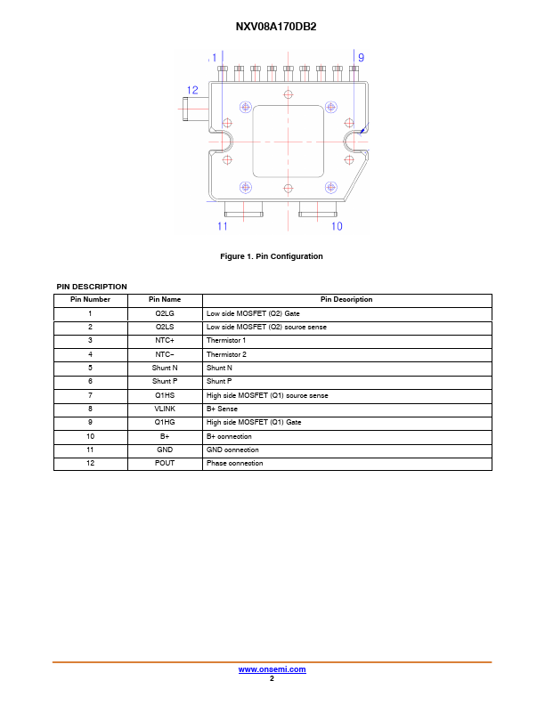
Pin Number 1 2 3 4 5 6 7 8 9 10 11 12
Pin Name Q2LG Q2LS NTC+ NTC
Shunt N Shunt P Q1HS VLINK Q1HG B+ GND POUT
Figure 1. Pin Configuration
Pin Description Low side MOSFET (Q2) Gate Low side MOSFET (Q2) source sense Thermistor 1 Thermistor 2 Shunt N Shunt P High side MOSFET (Q1) source sense B+ Sense High side MOSFET (Q1) Gate B+ connection GND connection Phase connection
www.onsemi.com 2
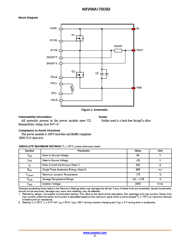
Block Diagram
NXV08A170DB2
VLINK Q1
Q1HG
Q1HS SHUNT P SHUNT N
Q2 Q2LG NTC+
NTC
Q2LS
B
Features
- Half Bridge Inverter for Variable Speed Motor Drive.
- Current Sensing and Temperature Sensing.
- Electrically Isolated DBC Substrate for Low Thermal Resistance.
- Compact Design for Low Total Module Resistance.
- Module Serialization for Full Traceability.
- C Snubber for Low EMI.
- AQG324 Qualified.
- PPAP Capable.
- This Device is Pb.
- free, RoHS and UL94.
- V0 Compliant.
 NXV08A170DB2-ONSemiconductor.pdf