Datasheet Details
| Part number | SCY99376 |
|---|---|
| Manufacturer | ON Semiconductor |
| File Size | 0.98 MB |
| Description | LDO Regulator |
| Datasheet |
 SCY99376 Datasheet SCY99376 Datasheet
|
|
|
| Part number | SCY99376 |
|---|---|
| Manufacturer | ON Semiconductor |
| File Size | 0.98 MB |
| Description | LDO Regulator |
| Datasheet |
SCY99376 Datasheet
|
|
|
|
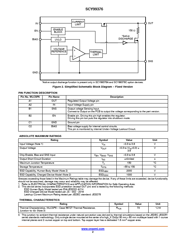
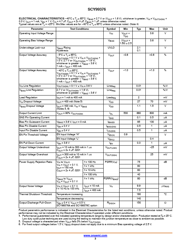
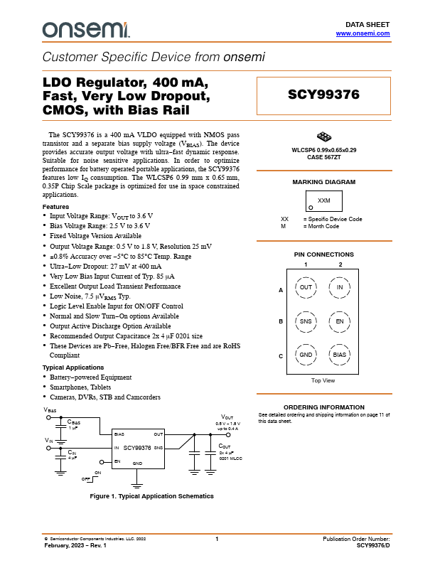
Pin No. Voltage Loc