PI6C2405A
PI6C2405A is Zero-Delay Clock Buffer manufactured by Pericom Semiconductor.
Features
- -
- -
- -
- - Maximum rated frequency: 133 MHz Low cycle-to-cycle jitter Input to output delay, less than 300ps Internal feedback allows outputs to be synchronized to the clock input 5V tolerant input- Spread spectrum clock ready Operates at 3.3V VDD Packaging (Pb-free & Green available): -8-pin, 150-mil SOIC (W) -8-pin, 173-mil TSSOP (L)
Description
The PI6C2405A is a PLL based, zero-delay buffer, with the ability to distribute five outputs of up to 133MHz at 3.3V. All the outputs are distributed from a single clock input CLKIN and output OUT0 performs zero delay by connecting a feedback to PLL. An internal feedback on OUT0 is used to synchronize the outputs to the input; the relationship between loading of this signal and the outputs determines the input-output delay. PI6C2405A is able to track spread spectrum clocking for EMI reduction. PI6C2405A is characterized for both mercial and industrial operation. PI6C2405A-1H is a high-drive version of PI6C2405A-1
- CLKIN must reference the same voltage thresholds for the PLL to deliver zero delay skewing
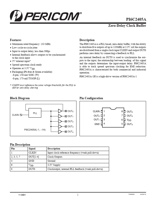
Block Diagram
Pin Configuration
CLKIN
OUT0 OUT1 OUT2 OUT3
CLKIN OUT2 OUT1 GND
1 2 3 4
8 7 6 5
OUT0 OUT4 VDD OUT3
PI6C2405A(- 1,
- 1H)
OUT4
Pin Description
Pin 1 2, 3, 5, 7 4 6 8 Signal CLKIN OUT[1-4] GND VDD OUT0 Description
Input clock reference frequency (weak pull-down) Clock Outputs Ground 3.3V Supply Clockoutput, internal PLL feedback (weak pull-down)
PS8592D
09/22/04
PI6C2405A Zero Delay Clock Buffer Zero Delay and Skew Control
CLKIN
- Input to OUTx Delay (ps)
CLKIN Input to OUTx Delay vs. Difference in Loading between OUT0 pin and OUTx pins
600 400 200 0 -200 -400 -600 -800
-25 -20 -15 -10 -5 0 5 10 15 20 25
PI6C2405A-1H
-900
PI6C2405A-1
-1000
Output Load Difference: OUT0 Load
- OUTx Load (p F)
The relationship between loading of the OUT0 signal and other outputs determines the input-output delay. Zero delay is achieved when all outputs, including feedback, are loaded...