Datasheet Details
| Part number | RD74LVC1G79 |
|---|---|
| Manufacturer | Renesas Technology |
| File Size | 2.03 MB |
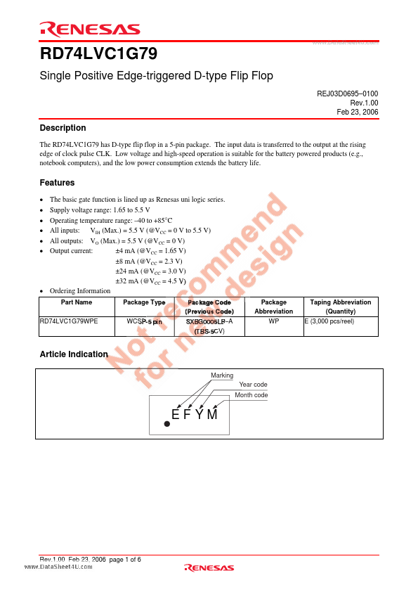
| Description | Single Positive Edge-triggered D-type Flip Flop |
| Datasheet |
 RD74LVC1G79 Datasheet RD74LVC1G79 Datasheet
|
|
|
| Part number | RD74LVC1G79 |
|---|---|
| Manufacturer | Renesas Technology |
| File Size | 2.03 MB |
| Description | Single Positive Edge-triggered D-type Flip Flop |
| Datasheet |
RD74LVC1G79 Datasheet
|
|
|
|
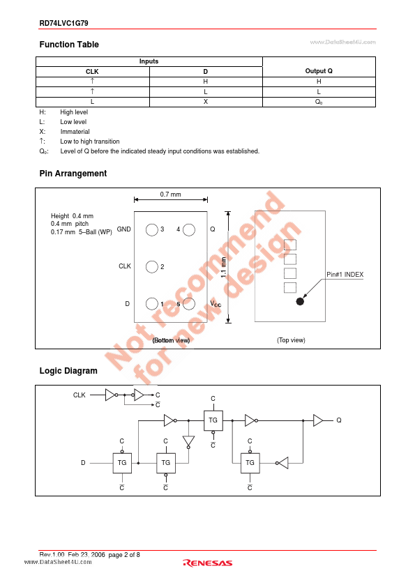
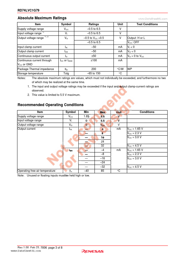
The RD74LVC1G79 has D-type flip flop in a 5-pin package.
📁 Similar Datasheet