Datasheet4U Logo Datasheet4U.com

RD74LVC2G17 Dual Schmitt-trigger Buffers

📥 Download Datasheet  Datasheet Preview Page 1

Description

RD74LVC2G17 Dual Schmitt-trigger Buffers REJ03D0757 *0100 Rev.1.00 Jul 26, 2006 .
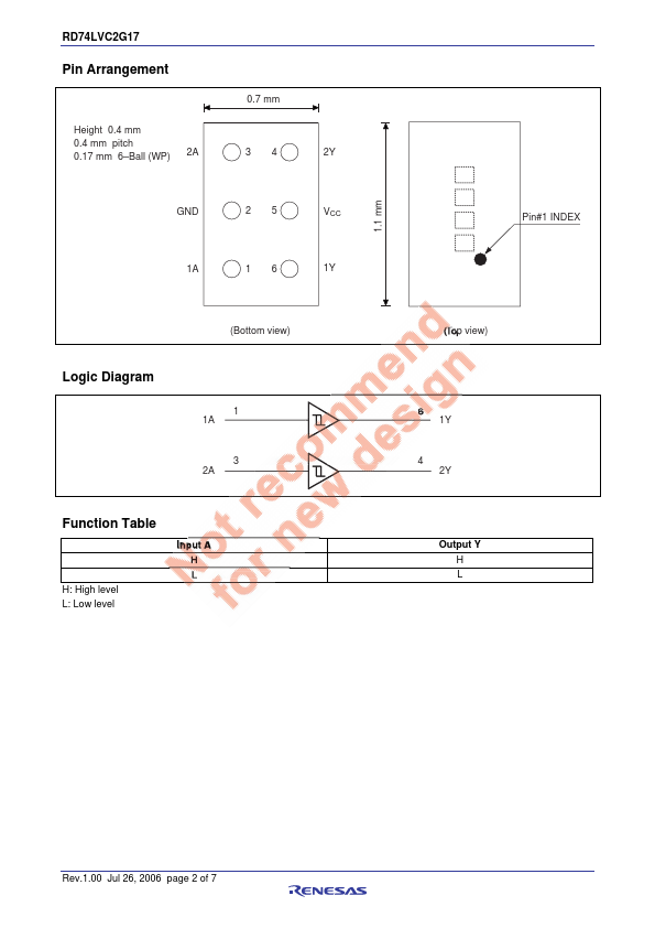
The RD74LVC2G17 has Dual Schmitt-trigger buffer in a 6-pin package.

📥 Download Datasheet

Preview of RD74LVC2G17 PDF
datasheet Preview Page 2 datasheet Preview Page 3

Features

* The basic gate function is lined up as Renesas uni logic series.
* Supply voltage range : 1.65 to 5.5 V
* Operating temperature range:
* 40 to +85°C
* All inputs: VIH (Max. ) = 5.5 V (@VCC = 0 V to 5.5 V)
* All outputs: VO (Max. ) = 5.5 V (@VCC = 0 V

RD74LVC2G17 Distributors

📁 Related Datasheet

  • RD74LVC00B - Quad 2-input NAND Gates (Renesas Technology)
  • RD74LVC125B - Quad. Bus Buffer Gates (Renesas Technology)
  • RD74LVC126B - Quad. Bus Buffer Gates (Renesas Technology)
  • RD74LVC138B - 3-to-8-line Decoder / Demultiplexer (Renesas Technology)
  • RD74LVC139B - Dual 2-to-4-line Decoders / Demultiplexers (Renesas Technology)
  • RD74LVC14B - Hex Schmitt-trigger Inverters (Renesas Technology)

📌 All Tags

Renesas RD74LVC2G17-like datasheet