Datasheet4U Logo Datasheet4U.com

RD74LVC126B Datasheet - Renesas Technology

Quad. Bus Buffer Gates

RD74LVC126B Features

* VCC = 1.65 V to 5.5 V All inputs VIH (Max.) = 5.5 V (@VCC = 0 V to 5.5 V) All outputs VOUT (Max.) = 5.5 V (@VCC = 0 V or output off state) Typical VOL ground bounce < 0.8 V (@VCC = 3.3 V, Ta = 25°C) Typical VOH undershoot > 2.0 V (@VCC = 3.3 V, Ta = 25°C) High output current ±4 mA (@VCC = 1.65 V) ±8

RD74LVC126B General Description

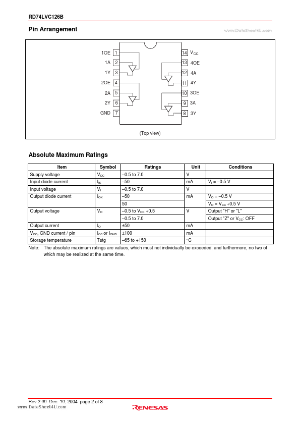
The RD74LVC126B has four bus buffer gates in a 14 pin package. The device requires the three state control input OE to be taken low to put the output into the high impedance condition. Low voltage and high-speed operation is suitable at the battery drive product (note type personal computer) and low.

RD74LVC126B Datasheet (124.92 KB)

Preview of RD74LVC126B PDF

Datasheet Details

Part number:

RD74LVC126B

Manufacturer:

Renesas ↗ Technology

File Size:

124.92 KB

Description:

Quad. bus buffer gates.

📁 Related Datasheet

RD74LVC125B Quad. Bus Buffer Gates (Renesas Technology)

RD74LVC138B 3-to-8-line Decoder / Demultiplexer (Renesas Technology)

RD74LVC139B Dual 2-to-4-line Decoders / Demultiplexers (Renesas Technology)

RD74LVC14B Hex Schmitt-trigger Inverters (Renesas Technology)

RD74LVC16240B 16-bit Buffers / Line Drivers (Renesas Technology)

RD74LVC16244B 16-bit Buffers / Line Drivers (Renesas Technology)

RD74LVC16245B 16-bit Bus Transceivers (Renesas Technology)

RD74LVC16373B 16-bit D-type Transparent Latches (Renesas Technology)

RD74LVC16374B 16-bit D-type Flip Flops (Renesas Technology)

RD74LVC1G00 2-input NAND Gate (Renesas Technology)

TAGS

RD74LVC126B Quad. Bus Buffer Gates Renesas Technology

Image Gallery

RD74LVC126B Datasheet Preview Page 2 RD74LVC126B Datasheet Preview Page 3

RD74LVC126B Distributor