Datasheet4U Logo Datasheet4U.com

RD74LVC138B Datasheet - Renesas Technology

3-to-8-line Decoder / Demultiplexer

RD74LVC138B Features

* VCC = 1.65 V to 5.5 V All inputs VIH (Max.) = 5.5 V (@VCC = 0 V to 5.5 V) Typical VOL ground bounce < 0.8 V (@VCC = 3.3 V, Ta = 25°C) Typical VOH undershoot > 2.0 V (@VCC = 3.3 V, Ta = 25°C) High output current ±4 mA (@VCC = 1.65 V) ±8 mA (@VCC = 2.3 V) ±12 mA (@VCC = 2.7 V) ±24 mA (@VCC = 3.0 V to

RD74LVC138B General Description

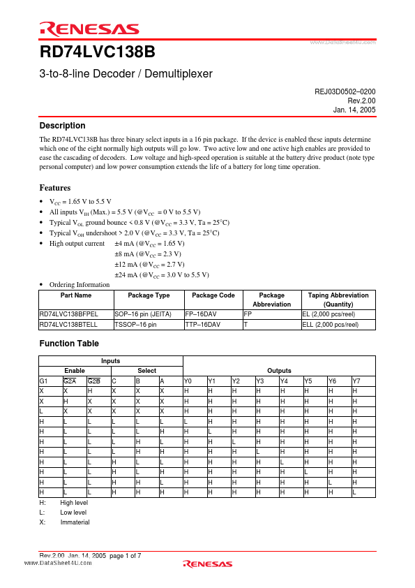
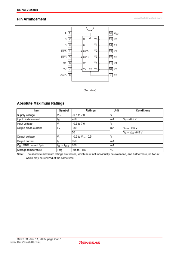
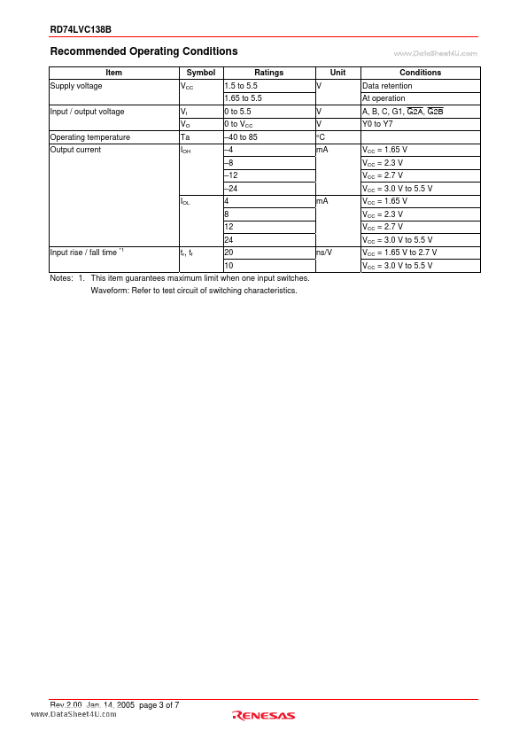
The RD74LVC138B has three binary select inputs in a 16 pin package. If the device is enabled these inputs determine which one of the eight normally high outputs will go low. Two active low and one active high enables are provided to ease the cascading of decoders. Low voltage and high-speed operatio.

RD74LVC138B Datasheet (96.21 KB)

Preview of RD74LVC138B PDF

Datasheet Details

Part number:

RD74LVC138B

Manufacturer:

Renesas ↗ Technology

File Size:

96.21 KB

Description:

3-to-8-line decoder / demultiplexer.

📁 Related Datasheet

RD74LVC139B Dual 2-to-4-line Decoders / Demultiplexers (Renesas Technology)

RD74LVC125B Quad. Bus Buffer Gates (Renesas Technology)

RD74LVC126B Quad. Bus Buffer Gates (Renesas Technology)

RD74LVC14B Hex Schmitt-trigger Inverters (Renesas Technology)

RD74LVC16240B 16-bit Buffers / Line Drivers (Renesas Technology)

RD74LVC16244B 16-bit Buffers / Line Drivers (Renesas Technology)

RD74LVC16245B 16-bit Bus Transceivers (Renesas Technology)

RD74LVC16373B 16-bit D-type Transparent Latches (Renesas Technology)

RD74LVC16374B 16-bit D-type Flip Flops (Renesas Technology)

RD74LVC1G00 2-input NAND Gate (Renesas Technology)

TAGS

RD74LVC138B 3-to-8-line Decoder Demultiplexer Renesas Technology

Image Gallery

RD74LVC138B Datasheet Preview Page 2 RD74LVC138B Datasheet Preview Page 3

RD74LVC138B Distributor