Datasheet4U Logo Datasheet4U.com

RD74LVC1G98

Configurable Multiple-Function Gate

RD74LVC1G98 Features

* The basic gate function is lined up as Renesas uni logic series. Supply voltage range: 1.65 to 5.5 V Operating temperature range:

* 40 to +85°C All inputs VIH (Max.) = 5.5 V (@VCC = 0 V to 5.5 V) All outputs VO (Max.) = 5.5 V (@VCC = 0 V) Output current: ±4 mA (@VCC = 1.65 V) ±8 mA (@VCC = 2.

RD74LVC1G98 General Description

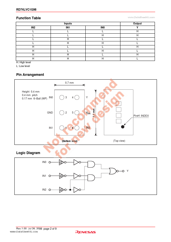
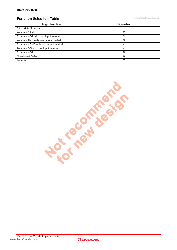
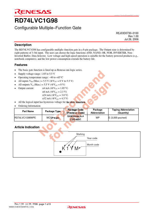
The RD74LVC1G98 has configurable multiple *function gate in a 6-pin package. The Output state is determined by eight patterns of 3 *bit input. The user can choose the logic functions AND, NAND, OR, NOR, INVERTER, Non * Inverted Buffer, Data Selector. Low voltage and high-speed o.

RD74LVC1G98 Datasheet (2.11 MB)

Preview of RD74LVC1G98 PDF

Datasheet Details

Part number:

RD74LVC1G98

Manufacturer:

Renesas ↗ Technology

File Size:

2.11 MB

Description:

Configurable multiple-function gate.

📁 Related Datasheet

RD74LVC1G00 2-input NAND Gate (Renesas Technology)

RD74LVC1G02 2-input NOR Gate (Renesas Technology)

RD74LVC1G04 Inverter (Renesas Technology)

RD74LVC1G07 Single Buffer / Driver with Open Drain (Renesas Technology)

RD74LVC1G08 2-input AND Gate (Renesas Technology)

RD74LVC1G125 Bus Buffer (Renesas Technology)

RD74LVC1G126 Bus Buffer (Renesas Technology)

RD74LVC1G14 Schmitt-trigger Inverter Buffer (Renesas Technology)

RD74LVC1G17 Schmitt-trigger Buffer (Renesas Technology)

RD74LVC1G240 Bus Buffer Inverted (Renesas Technology)

TAGS

RD74LVC1G98 Configurable Multiple-Function Gate Renesas Technology

Image Gallery

RD74LVC1G98 Datasheet Preview Page 2 RD74LVC1G98 Datasheet Preview Page 3

RD74LVC1G98 Distributor