Datasheet Details
| Part number | 5PB1108PGG |
|---|---|
| Manufacturer | Renesas |
| File Size | 1.99 MB |
| Description | 1.8V to 3.3V High-Performance LVCMOS Clock Buffer |
| Datasheet | 5PB1108PGG 5PB1102PGG Datasheet (PDF) |
|
|
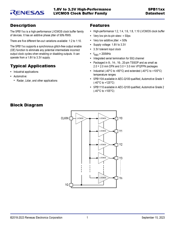
Overview: 1.8V to 3.3V High-Performance LVCMOS Clock Buffer Family 5PB11xx.
This datasheet includes multiple variants, all published together in a single manufacturer document.
| Part number | 5PB1108PGG |
|---|---|
| Manufacturer | Renesas |
| File Size | 1.99 MB |
| Description | 1.8V to 3.3V High-Performance LVCMOS Clock Buffer |
| Datasheet | 5PB1108PGG 5PB1102PGG Datasheet (PDF) |
|
|
|
The 5PB11xx is a high-performance LVCMOS clock buffer family of devices.
It has an additive phase jitter of 50fs RMS.
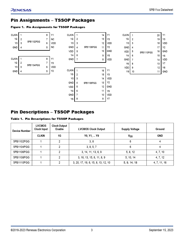
There are five different fan-out variations available: 1:2 to 1:10.
| Brand Logo | Part Number | Description | Other Manufacturers |
|---|---|---|---|
| 5PB1108PGG | 1.8V to 3.3V LVCMOS High-Performance Clock Buffer | IDT | |
| 5PB1108PGGI | 1.8V to 3.3V LVCMOS High Performance Clock Buffer | IDT | |
| 5PB1108CMGI | 1.8V to 3.3V LVCMOS High Performance Clock Buffer | IDT |
| Part Number | Description |
|---|---|
| 5PB1108PGGI | 1.8V to 3.3V High-Performance LVCMOS Clock Buffer |
| 5PB1108CMG | 1.8V to 3.3V High-Performance LVCMOS Clock Buffer |
| 5PB1102CMG | 1.8V to 3.3V High-Performance LVCMOS Clock Buffer |
| 5PB1102CMGI | 1.8V to 3.3V High-Performance LVCMOS Clock Buffer |
| 5PB1102PGG | 1.8V to 3.3V High-Performance LVCMOS Clock Buffer |
| 5PB1102PGGI | 1.8V to 3.3V High-Performance LVCMOS Clock Buffer |
| 5PB1104 | 1.8V to 3.3V High-Performance LVCMOS Clock Buffer |
| 5PB1104CMG | 1.8V to 3.3V High-Performance LVCMOS Clock Buffer |
| 5PB1104CMGI | 1.8V to 3.3V High-Performance LVCMOS Clock Buffer |
| 5PB1104CMT | 1.8V to 3.3V High-Performance LVCMOS Clock Buffer |