Datasheet4U Logo Datasheet4U.com

9DB436 Datasheet - Renesas

4-Output 3.3V HCSL PCIe Buffer

9DB436 Features

* ▪ Four 0.7V current-mode differential HCSL output pairs ▪ Supports zero delay buffer (ZDB) mode and fanout mode ▪ Selectable bandwidth for zero delay mode ▪ 50

* 110 MHz operation in PLL mode ▪ 5

* 166 MHz operation in Bypass mode Features ▪ SPS internal receiver bias network keeps inpu

9DB436 General Description

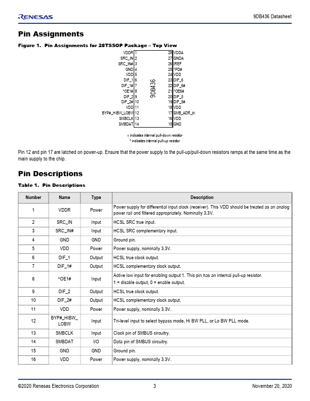
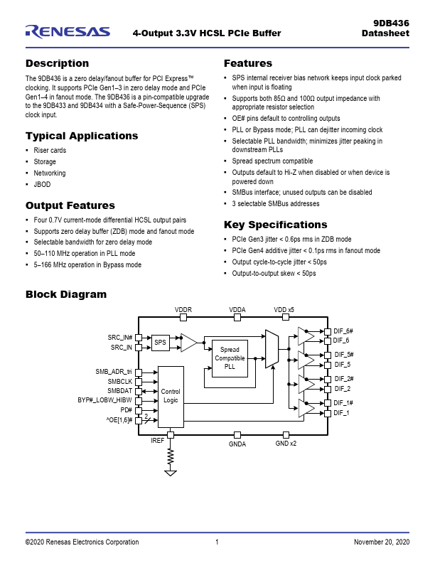
The 9DB436 is a zero delay/fanout buffer for PCI Express™ clocking. It supports PCIe Gen1 *3 in zero delay mode and PCIe Gen1 *4 in fanout mode. The 9DB436 is a pin-compatible upgrade to the 9DB433 and 9DB434 with a Safe-Power-Sequence (SPS) clock input. Typical Applications ▪ Riser ca.

9DB436 Datasheet (366.55 KB)

Preview of 9DB436 PDF

Datasheet Details

Part number:

9DB436

Manufacturer:

Renesas ↗

File Size:

366.55 KB

Description:

4-output 3.3v hcsl pcie buffer.

📁 Related Datasheet

9DB433 FOUR OUTPUT DIFFERENTIAL BUFFER (IDT)

9DB433 FOUR OUTPUT DIFFERENTIAL BUFFER (Renesas)

9DB401C Four Output Differential Buffer (Renesas)

9DB423B Four Output Differential Buffer (IDT)

9DB423B 4-OUTPUT DIFFERENTIAL BUFFER (Renesas)

9DB106 Six Output Differential Buffer (IDT)

9DB106 Six Output Differential Buffer (Renesas)

9DB1200C Twelve Output Differential Buffer (IDT)

9DB1200C Twelve Output Differential Buffer (Renesas)

9DB1233 Twelve Output Differential Buffer (IDT)

TAGS

9DB436 4-Output 3.3V HCSL PCIe Buffer Renesas

Image Gallery

9DB436 Datasheet Preview Page 2 9DB436 Datasheet Preview Page 3

9DB436 Distributor