Datasheet Details
- Part number
- ISL89367
- Manufacturer
- Renesas ↗
- File Size
- 665.31 KB
- Datasheet
- ISL89367-Renesas.pdf
- Description
- MOSFET Driver
ISL89367 Description
ISL89367 NOT RECOMMENDED FOR NEW DESIGNS NO RECOMMENDED REPLACEMENT contact our Technical Support Center at 1-888-INTERSIL or www.intersil.com/tsc H.
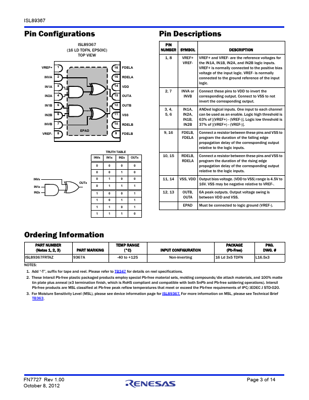
PIN NUMBER SYMBOL
DESCRIPTION
1, 8 VREF+ VREF+ and VREF- are the reference voltages for VREF- the IN1A, IN1B, IN2A, and IN2B logic inputs.
ISL89367 Features
* 2 outputs with 6A peak drive currents (sink and source) with output voltage range of 4.5V to 16V
* Typical ON-resistance
ISL89367 Applications
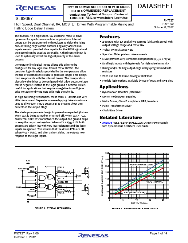
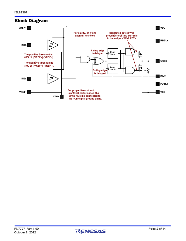
* Internal timers can be programmed with resistors to delay the rising and/or falling edges of the outputs. Logically ANDed dual inputs are also provided. One input is for the PWM signal and the second can be used as an enable. A third control input is used to optionally invert the logical polarity o
📁 Related Datasheet
📌 All Tags
ISL89367 Stock/Price