Click to expand full text
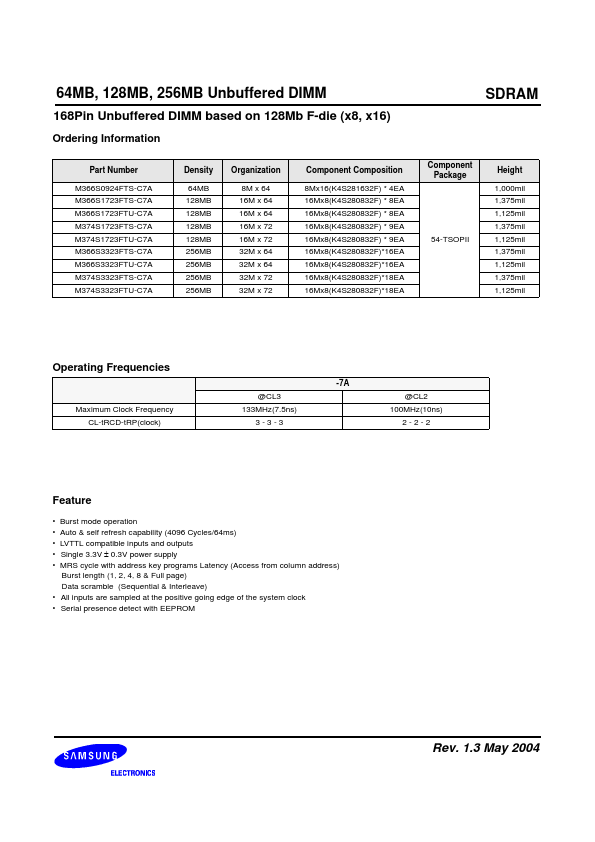
64MB, 128MB, 256MB Unbuffered DIMM
SDRAM
SDRAM Unbuffered Module
168pin Unbuffered Module based on 128Mb F-die 62/72-bit Non ECC/ECC
Revision 1.3 May 2004
* Samsung Electronics reserves the right to change products or specification without notice.
Rev. 1.3 May 2004
64MB, 128MB, 256MB Unbuffered DIMM
Revision History
Revision 0.0 (November, 2003) - First release Revision 1.0 (January, 2004) - Revision 1.0 spec release. Revision 1.1 (February, 2004) - Corrected typo. Revision 1.2 (March. 2004) - Modified DC Characteristics Notes. Revision 1.3 (May, 2004) - Added Note 5. sentense of tRDL parameter
SDRAM
Rev. 1.
 M374S3323FTU-C7A Datasheet