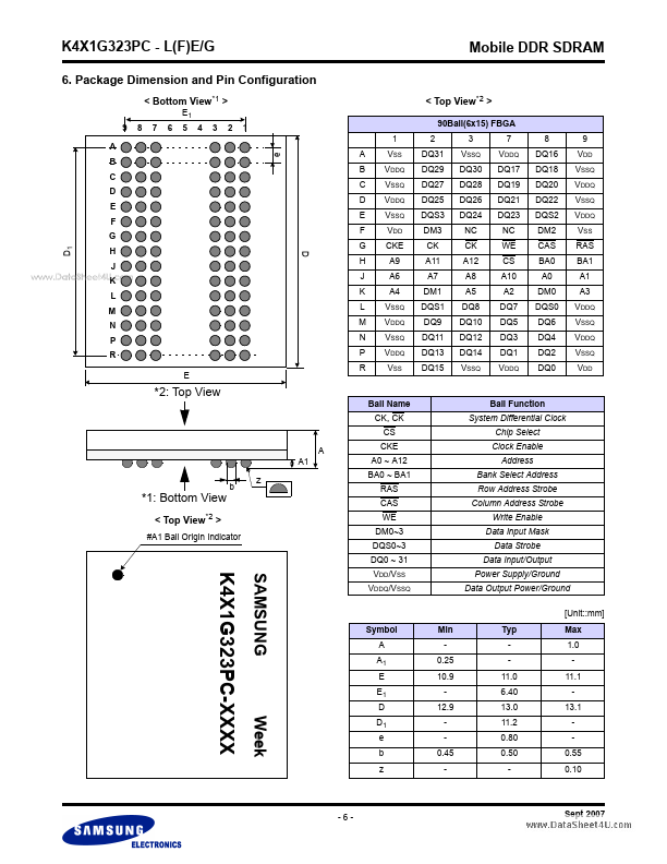
Description
Symbol CK, CK Type Input Description
Mobile DDR SDRAM
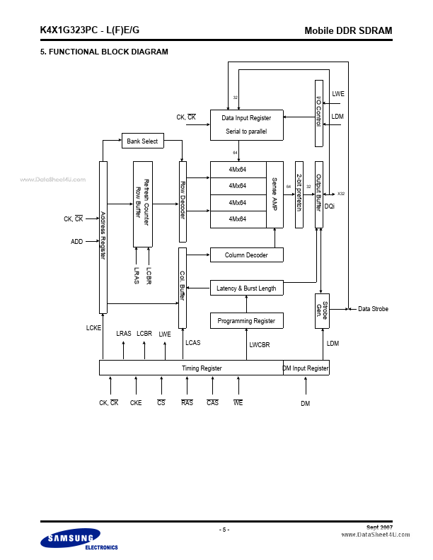
Clock : CK and CK are differential clock inputs.All address and control input signals are sampled on the crossing of the positive edge of CK and negative edge of CK.Internal clock signals are derived from CK/CK.Clock Enable : CKE HIGH activates, and CKE LOW deactivates internal clock signals, and device input buffers and output drivers.Taking CKE LOW provides PRECHARGE POWER-DOWN and SELF REFRESH operation (all banks idle), or ACTIVE PO
Features
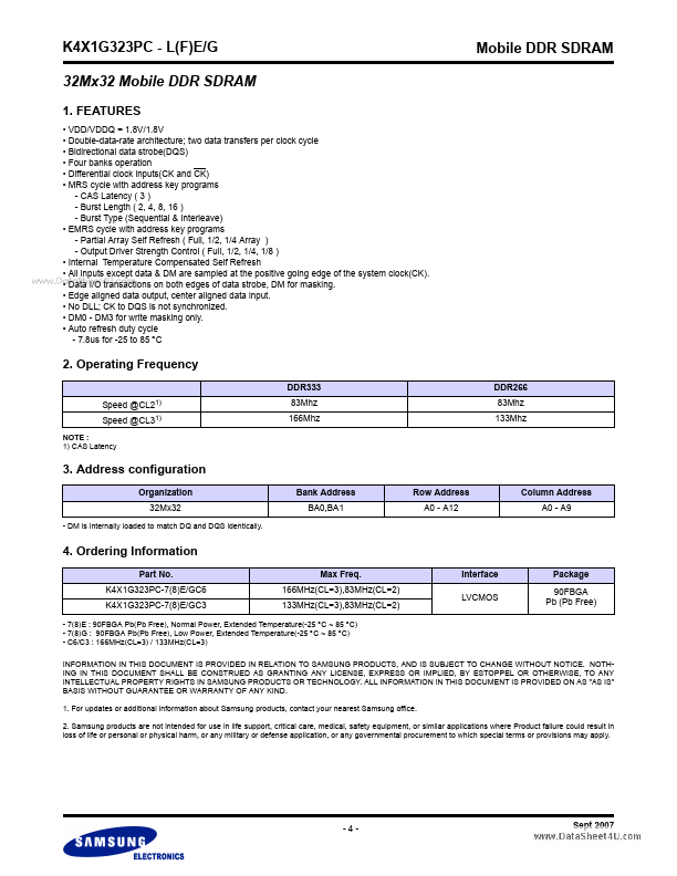
- VDD/VDDQ = 1.8V/1.8V.
- Double-data-rate architecture; two data transfers per clock cycle.
- Bidirectional data strobe(DQS).
- Four banks operation.
- Differential clock inputs(CK and CK).
- MRS cycle with address key programs - CAS Latency ( 3 ) - Burst Length ( 2, 4, 8, 16 ) - Burst Type (Sequential & Interleave).
- EMRS cycle with address key programs - Partial Array Self Refresh ( Full, 1/2, 1/4 Array ) - Output Driver Strength Control ( Fu.
 K4X1G323PC-L_Samsungsemiconductor.pdf