Description
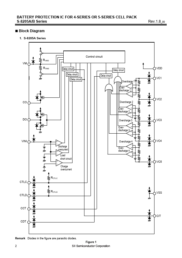
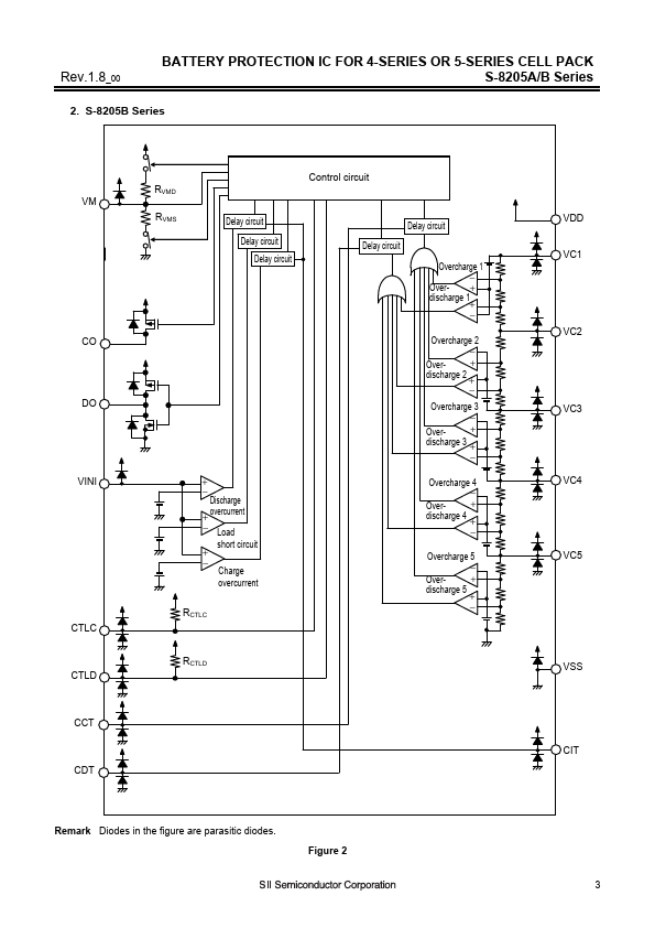
Pin for voltage detection between VSS pin and VM pin FET gate connection pin for charge control (Pch open-drain output) Pin for voltage detection between VSS pin and CO pin FET gate connection pin for discharge control FET (CMOS output) Pin for voltage detection between VSS pin and VINI pin Control pin for charge FET Control pin for discharge FET Capacitor connection pin for delay for overcharge detection voltage Capacitor connection pin for delay for overdischarge detection voltage Capacitor co
Features
- High-accuracy voltage detection function for each cell
Overcharge detection voltage n (n = 1 to 5)
3.55 V to 4.50 V.
- 1 (50 mV step)
Overcharge release voltage n (n = 1 to 5)
3.30 V to 4.50 V.
- 2
Overdischarge detection voltage n (n = 1 to 5)
2.0 V to 3.2 V.
- 1 (100 mV step)
Overdischarge release voltage n (n = 1 to 5)
2.0 V to 3.4 V.
- 3
Accuracy ±25 mV Accuracy ±50 mV Accuracy ±80 mV Accuracy ±100 mV.
- Discharge overcurrent detection in 2-step Discharge ove.
 S-8205A-Seiko.pdf