Datasheet4U Logo Datasheet4U.com

LH28F008SA - 8M (1M x 8) Flash Memory

Datasheet Summary

Description

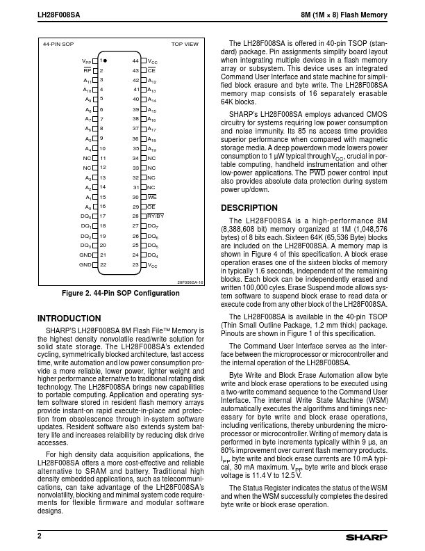
The LH28F008SA is a high-performance 8M (8,388,608 bit) memory organized at 1M (1,048,576 bytes) of 8 bits each.

Sixteen 64K (65,536 Byte) blocks are included on the LH28F008SA.

A memory map is shown in Figure 4 of this specification.

Features

  • 40-PIN TSOP 8M (1M × 8) Flash Memory TOP VIEW.
  • Very High-Performance Read.
  • 85 ns Maximum Access Time A19 A18 A17 A16 A15 A14 A13 A12 CE VCC VPP PWD A11 A10 A9 A8 A7 A6 A5 A4 1 2 3 4 5 6 7 8 9 10 11 12 13 14 15 16 17 18 19 20 40 39 38 37 36 35 34 33 32 31 30 29 28 27 26 25 24 23 22 21 NC NC WE OE RY/BY DQ7 DQ6 DQ5 DQ4 VCC GND GND DQ3 DQ2 DQ1 DQ0 A0 A1 A2 A3.
  • High-Density Symmetrically Blocked Architecture.
  • Sixteen 64K Blocks.
  • Extended Cycling Capab.

📥 Download Datasheet

Datasheet preview – LH28F008SA

Datasheet Details

Part number LH28F008SA
Manufacturer Sharp
File Size 249.75 KB
Description 8M (1M x 8) Flash Memory
Datasheet download datasheet LH28F008SA Datasheet
Additional preview pages of the LH28F008SA datasheet.
Other Datasheets by Sharp

Full PDF Text Transcription

Click to expand full text
LH28F008SA FEATURES 40-PIN TSOP 8M (1M × 8) Flash Memory TOP VIEW • Very High-Performance Read – 85 ns Maximum Access Time A19 A18 A17 A16 A15 A14 A13 A12 CE VCC VPP PWD A11 A10 A9 A8 A7 A6 A5 A4 1 2 3 4 5 6 7 8 9 10 11 12 13 14 15 16 17 18 19 20 40 39 38 37 36 35 34 33 32 31 30 29 28 27 26 25 24 23 22 21 NC NC WE OE RY/BY DQ7 DQ6 DQ5 DQ4 VCC GND GND DQ3 DQ2 DQ1 DQ0 A0 A1 A2 A3 • High-Density Symmetrically Blocked Architecture – Sixteen 64K Blocks • Extended Cycling Capability – 100,000 Block Erase Cycles – 1.6 Million Block Erase Cycles per Chip • Automated Byte Write and Block Erase – Command User Interface – Status Register • System Performance Enhancements – RY  / » BY  » Status Output – Erase Suspend Capability • Deep-Powerdown Mode – 0.
Published: |