Datasheet Details
- Part number
- HYS64V4120GU
- Manufacturer
- Siemens
- File Size
- 72.85 KB
- Datasheet
- HYS64V4120GU_SiemensSemiconductorGroup.pdf
- Description
- 3.3V 4M x 64-Bit 2 BANK SDRAM Module 3.3V 4M x 72-Bit 2 BANK SDRAM Module
HYS64V4120GU Description
3.3V 4M x 64-Bit 2 BANK SDRAM Module 3.3V 4M x 72-Bit 2 BANK SDRAM Module 168 pin unbuffered DIMM Modules HYS64V4120GU-10 HYS72V4120GU-10 * .HYS64V4120GU Features
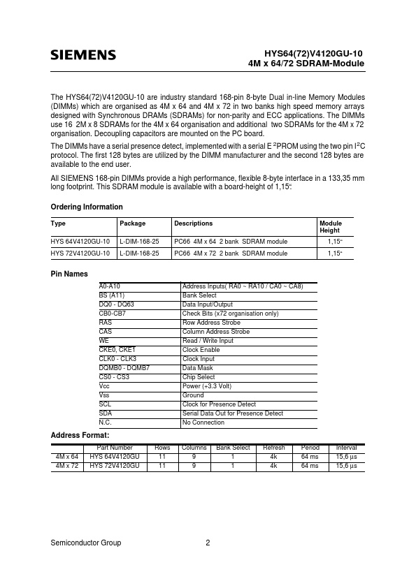
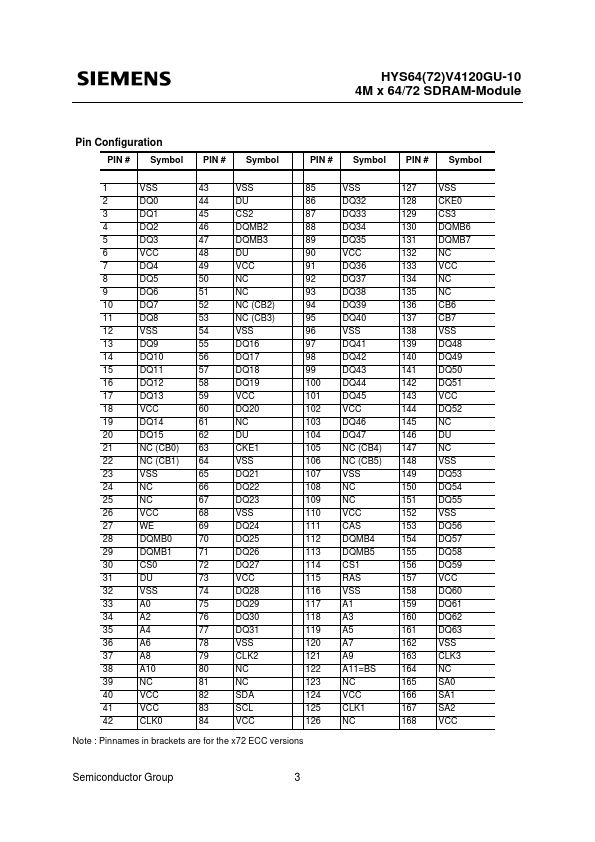
* s are registered on every rising clock edge during tRC(min). Values are shown per module bank. 2. The specified values are valid when data inputs (DQ’ s) are stable during tRC(min. ). 3. An initial pause of 100 µs is required after power-up, then a Precharge All Banks command must be given followed bHYS64V4120GU Applications
* 2 bank 4M x 64, 4M x 72 organisation Optimized for byte-write non-parity or ECC applications Fully PC66 layout compatible JEDEC standard Synchronous DRAMs (SDRAM) Performance: -10 fCK tAC Max. Clock frequency Max. access time from clock 66 MHz @ CL=2 100 MHz @ CL=3 9 ns @ CL=2 8 ns @ CL=3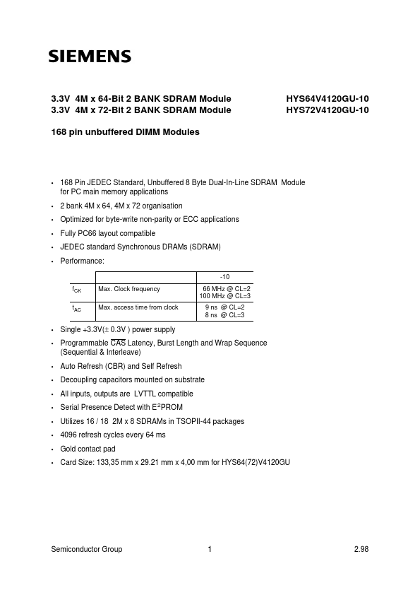
📁 Related Datasheet
📌 All Tags