Datasheet Details
| Part number | HYS72V2100GU-10 |
|---|---|
| Manufacturer | Siemens |
| File Size | 75.48 KB |
| Description | 3.3V 2M x 64-Bit SDRAM Module 3.3V 2M x 72-Bit SDRAM Module |
| Datasheet |
 HYS72V2100GU-10 Datasheet HYS72V2100GU-10 Datasheet
|
|
|
| Part number | HYS72V2100GU-10 |
|---|---|
| Manufacturer | Siemens |
| File Size | 75.48 KB |
| Description | 3.3V 2M x 64-Bit SDRAM Module 3.3V 2M x 72-Bit SDRAM Module |
| Datasheet |
HYS72V2100GU-10 Datasheet
|
|
|
|
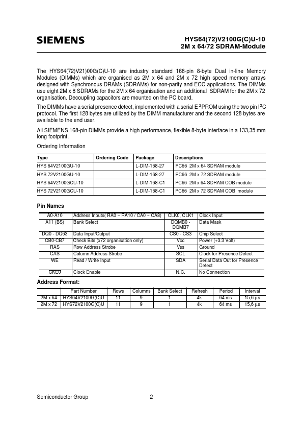
PC66 2M x 64 SDRAM module PC66 2M x 72 SDRAM module PC66 2M x 64 SDRAM COB module PC66 2M x 72 SDRAM COB module Pin Names A0-A10 A11 (BS) DQ0 - DQ63 CB0-CB7 RAS CAS WE CKE0 Address Inputs( RA0 ~ RA10 / CA0 ~ CA8) Bank Select Data Input/Output Check Bits (x72 organisation only) Row Address Strobe Column Address Strobe Read / Write Input Clock Enable CLK0, CLK1 DQMB0 DQMB7 CS0 - CS3 Vcc Vss SCL SDA N.C.Clock Input Data Mask Chip Select Power (+3.3 Volt) Ground Clock for Presence Detect Serial D
📁 Similar Datasheet