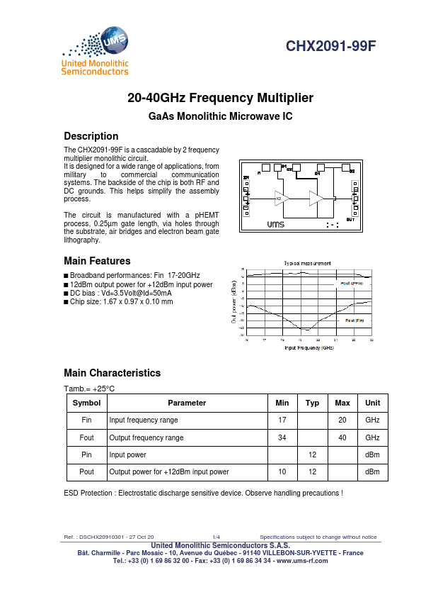
Description
The CHX2091-99F is a cascadable by 2 frequency
multiplier monolithic circuit.It is designed for a wide range of applications, from
military to commercial communication
systems.The backside of the chip is both RF and
DC grounds.This helps simplify the assembly
process.X2
The circuit is manufactured with a pHEMT process, 0.25µm gate length, via holes through the substrate, air bridges and electron beam gate lithography.Main
Features
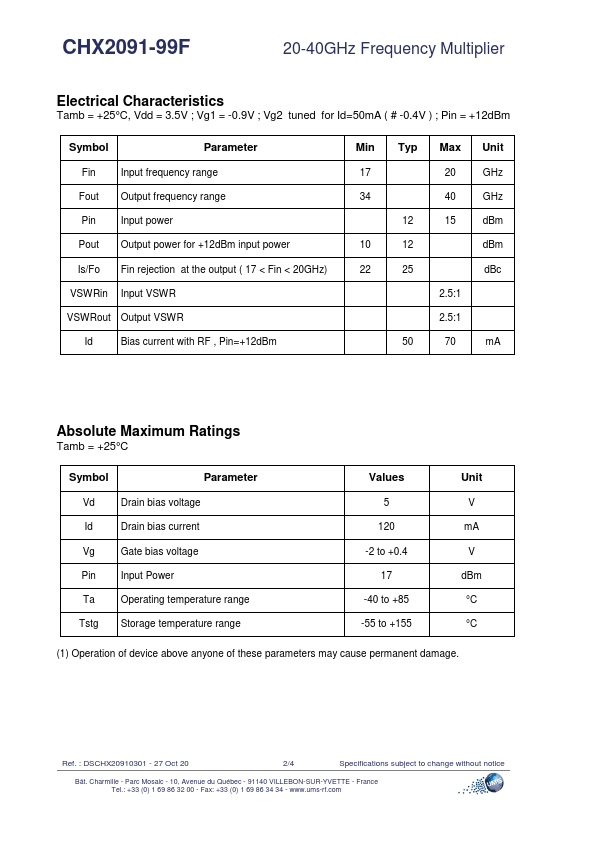
- Broadband performances: Fin 17-20GHz.
- 12dBm output power for +12dBm input power.
- DC bias : Vd=3.5Volt@Id=50mA.
- Chip size: 1.67 x 0.97 x 0.10 mm
Main Characteristics
Tamb. = +25°C
Symbol
Parameter
Fin Input frequency range
Fout Output frequency range
Pin Input power
Pout Output power for +12dBm input power
Min Typ Max Unit
17
20
GHz
34
40
GHz
12
dBm
10
12
dBm
ESD Protection : Electrostatic discharge sensitive device. Observe handling precautions !
Ref. :.
 CHX2091-99F-UnitedMonolithicSemiconductors.pdf