Datasheet Details
| Part number | V96BMC |
|---|---|
| Manufacturer | V3 Semiconductor |
| File Size | 127.41 KB |
| Description | High Performance Burst DRAM Controller |
| Datasheet |
 V96BMC_V3Semiconductor.pdf V96BMC_V3Semiconductor.pdf
|
| Part number | V96BMC |
|---|---|
| Manufacturer | V3 Semiconductor |
| File Size | 127.41 KB |
| Description | High Performance Burst DRAM Controller |
| Datasheet |
V96BMC_V3Semiconductor.pdf
|
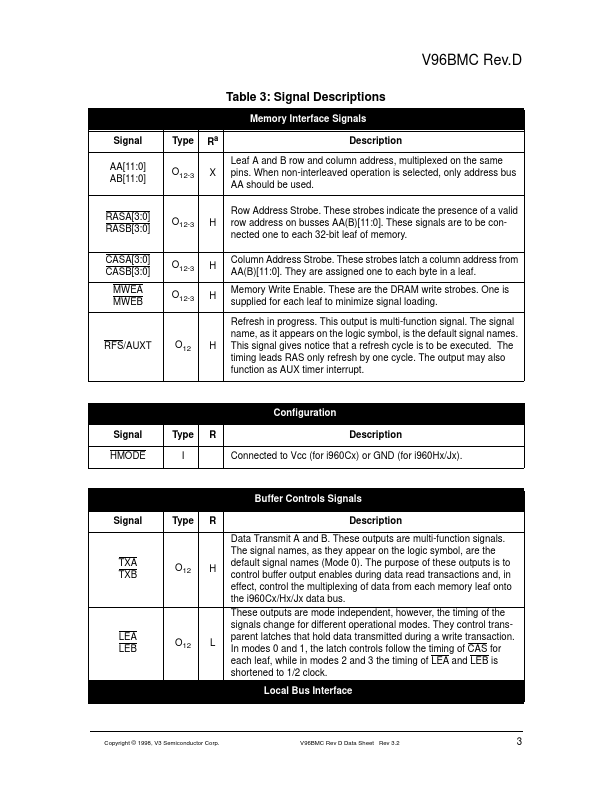
and Pinout Table 2 below lists the pin types found on the V96BMC.Table 3 describes the function of each pin on the V96BMC.Table 4 lists the pins by pin number.Figure 1 shows the pinout for the 132-pin PQFP package and Figure 2 shows the mechanical dimensions of the package.Table 2: Pin Types Pin Type I/O12 I O12 Description TTL I/O pin with 12 mA output drive TTL input only pin TTL Output pin with 12 mA output drive TTL Output pin with 12 mA output drive that can be configured for either 5
📁 V96BMC Similar Datasheet