Datasheet4U Logo Datasheet4U.com

EDI7F2328XDNSN - 8M x 32 / 2 x 8Mx 32 INTEL J3 BASED

Datasheet Summary

Description

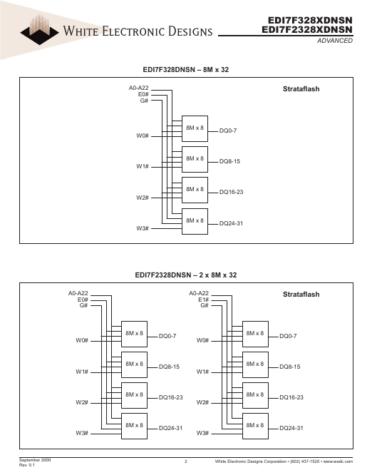
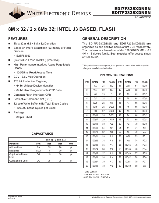
The EDI7F328XDNSN and EDI7F2328XDNSN are organized as one and two banks of 8M x 32 respectively.

The modules are based on Intel’s E28F640J3, 8M x 8 / 4M x 16 device family.

Both modules offer access times of 120-150ns.

Features

  • 8M x 32 and 2 x 8M x 32 Densities Based on Intel’s Strataflash (J3) family of Flash Devices.
  • E28F640J3 (64) 128Kb Erase Blocks (Symetrical) High Performance Interface Async Page Mode Reads.
  • 120/25 ns Read Access Time 2.7V - 3.6V Vcc Operation 128 bit Protection Register;.
  • 64 bit Unique Device Identifier.
  • 64 bit User Programmable OTP Cells Common Flash Interface (CFI) Scaleable Command Set (SCS) 32 byte Write Buffer, 64M Total Erase Cycles.
  • 100,000 Erase.

📥 Download Datasheet

Datasheet preview – EDI7F2328XDNSN

Datasheet Details

Part number EDI7F2328XDNSN
Manufacturer White Electronic Designs
File Size 144.53 KB
Description 8M x 32 / 2 x 8Mx 32 INTEL J3 BASED
Datasheet download datasheet EDI7F2328XDNSN Datasheet
Additional preview pages of the EDI7F2328XDNSN datasheet.
Other Datasheets by White Electronic Designs

Full PDF Text Transcription

Click to expand full text
www.DataSheet4U.com White Electronic Designs EDI7F328XDNSN EDI7F2328XDNSN ADVANCED* 8M x 32 / 2 x 8Mx 32; INTEL J3 BASED, FLASH FEATURES 8M x 32 and 2 x 8M x 32 Densities Based on Intel’s Strataflash (J3) family of Flash Devices • E28F640J3 (64) 128Kb Erase Blocks (Symetrical) High Performance Interface Async Page Mode Reads • 120/25 ns Read Access Time 2.7V - 3.
Published: |