Datasheet Details
| Part number | CSD25301W1015 |
|---|---|
| Manufacturer | Texas Instruments ↗ |
| File Size | 153.30 KB |
| Description | P-Channel Power MOSFET |
| Datasheet |
 CSD25301W1015-etcTI.pdf CSD25301W1015-etcTI.pdf
|
| Part number | CSD25301W1015 |
|---|---|
| Manufacturer | Texas Instruments ↗ |
| File Size | 153.30 KB |
| Description | P-Channel Power MOSFET |
| Datasheet |
CSD25301W1015-etcTI.pdf
|
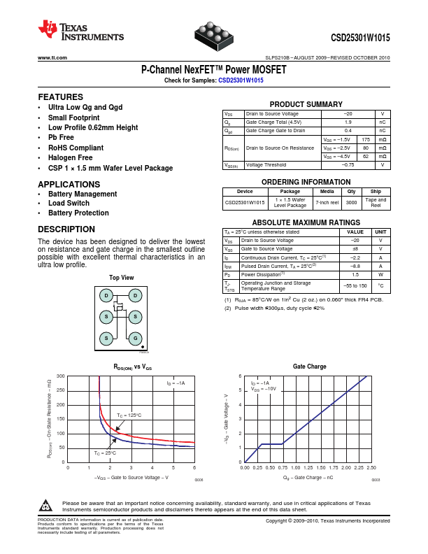
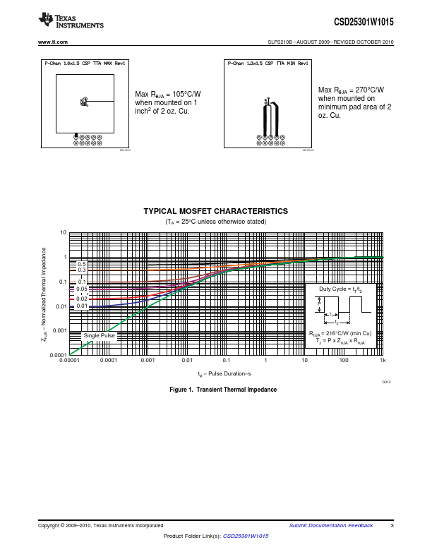
The device has been designed to deliver the lowest on resistance and gate charge in the smallest outline possible with excellent thermal characteristics in an ultra low profile. 20 V Qg Gate Charge Total (4.5V) 1.9 nC Qgd Gate Charge Gate to Drain 0.4 nC VGS = 1.5V 175 mΩ RDS(on) Drain to Source On Resistance VGS = 2.5V 80 mΩ VGS = 4.5V 62 mΩ VGS(th) Voltage Threshold
📁 CSD25301W1015 Similar Datasheet