Datasheet Details
| Part number | CSD25303W1015 |
|---|---|
| Manufacturer | Texas Instruments ↗ |
| File Size | 178.70 KB |
| Description | P-Channel Power MOSFET |
| Datasheet |
 CSD25303W1015-etcTI.pdf CSD25303W1015-etcTI.pdf
|
| Part number | CSD25303W1015 |
|---|---|
| Manufacturer | Texas Instruments ↗ |
| File Size | 178.70 KB |
| Description | P-Channel Power MOSFET |
| Datasheet |
CSD25303W1015-etcTI.pdf
|
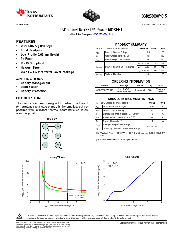
The device has been designed to deliver the lowest on resistance and gate charge in the smallest outline possible with excellent thermal characteristics in an ultra low profile. 20 3.3 0.6 VGS = 1.8V 72 VGS = 2.5V
📁 CSD25303W1015 Similar Datasheet